Highlights
- 8 notes
Highlights
- 8 notes
Highlight 1Assembling a laser cutter [note-0026]
- 07-05-2025
- noesis, with guidance from Paul Han
- #experimentalist-confetti
Highlight 1Assembling a laser cutter [note-0026]
- 07-05-2025
- noesis, with guidance from Paul Han
- #experimentalist-confetti
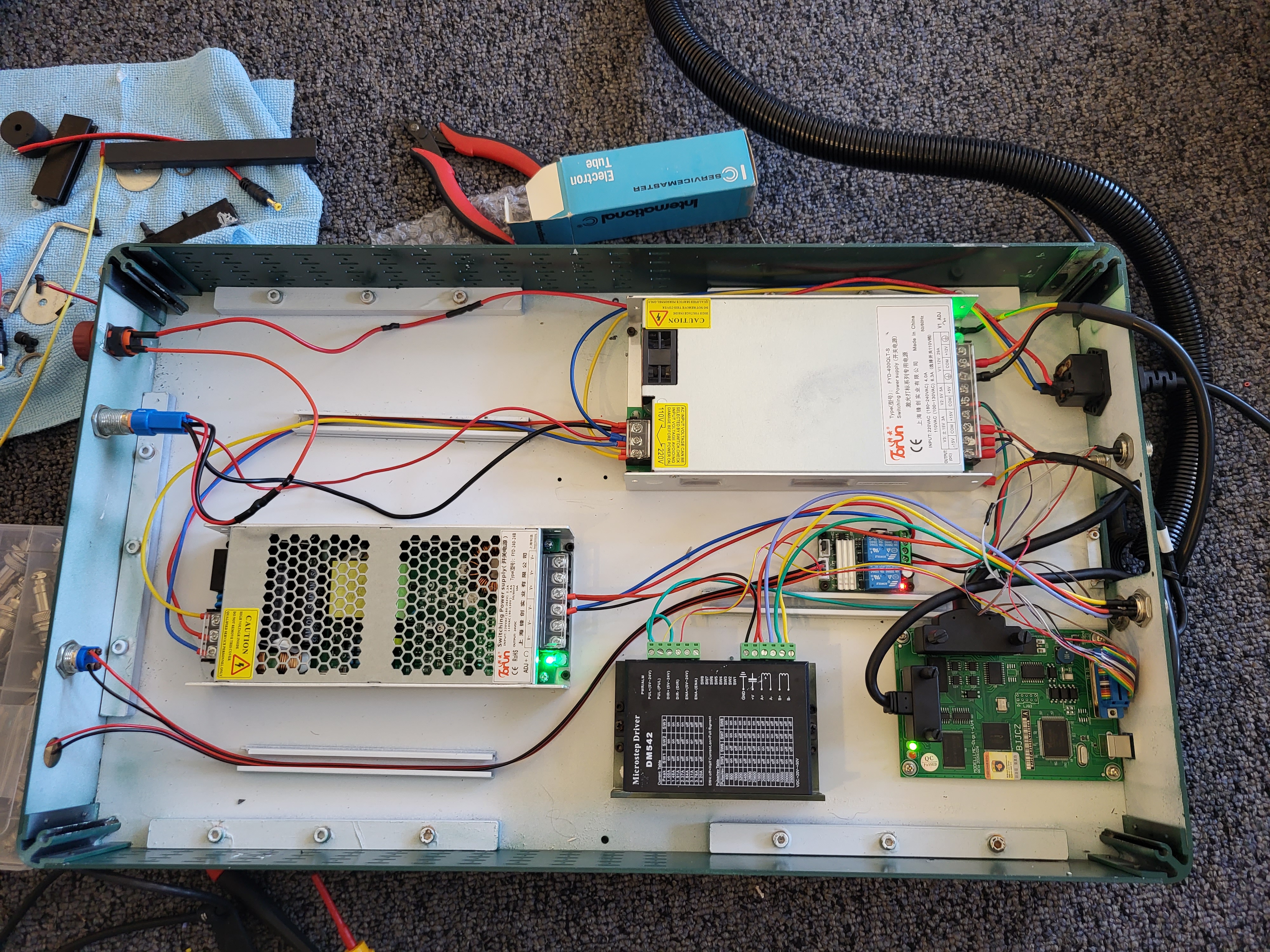
We accidentally spilled bleach on a CO2 laser cutter, so I got a chance to take it apart and reassemble it.
Highlight 2Arxiv wars [note-0001]
- 01-01-2025
- noesis
- #experimentalist-confetti
- #feral-scholars
- #autoresearch
Highlight 2Arxiv wars [note-0001]
- 01-01-2025
- noesis
- #experimentalist-confetti
- #feral-scholars
- #autoresearch
by: noesis, Joe and Cassandra from Prototype • 2025-03-16
Arxiv wars: Where simulated ML experts fight over the best real paper of the day! This takes place in an online forum, inspired by Hacker News with infinite backrooms aesthetics. Experts here included Joscha Bach, Yann LeCun, Sichu Lu and Alex K Chen!
Tech used: Python, React, Node.js, Express, MCP, ArXiv API,Discord
In the arguably 3rd iteration in Aug 2025, the context augmentation became RAG GitHub repo
Highlight 3Making low-cost microelectrode arrays [note-0012]
- 01-01-2025
- noesis and Eigenlucy
- #lab equipment
- #neuroscience
- #experimentalist-confetti
Highlight 3Making low-cost microelectrode arrays [note-0012]
- 01-01-2025
- noesis and Eigenlucy
- #lab equipment
- #neuroscience
- #experimentalist-confetti
3.1Motivation: Neuronal headstages bottlenecked researchers
3.1Motivation: Neuronal headstages bottlenecked researchers
2025 was full of startup hype about neuron computers. At Frontier Tower's neurotech floor, friends were discussing biological neuronal responses to nootropics and neuropeptides. However, the neuronal headstages were hard to get. Student clubs e.g. UC Berkeley didn't rent them out, nor did neurotech startups e.g. Science.xyz.
For reference, a single microelectrode array of 59 channels from multichannel systems costs $300.
Not to mention, integrated neuronal headstage setups from Axion biosystems cost $10k - $50k.
Thus, we experimented with building a cheap MEA, and so far graphene version costs <$1 and 5.5 min per unit.
3.2We tested 3 laser deposition techniques
3.2We tested 3 laser deposition techniques
- Laser-induced graphene
- Aluminum vapour deposition
- Copper metalization We've looked into laser ablation: Indium tin oxide. This was not tested but may also be worth a shot.
3.3Designing an MEA
3.3Designing an MEA
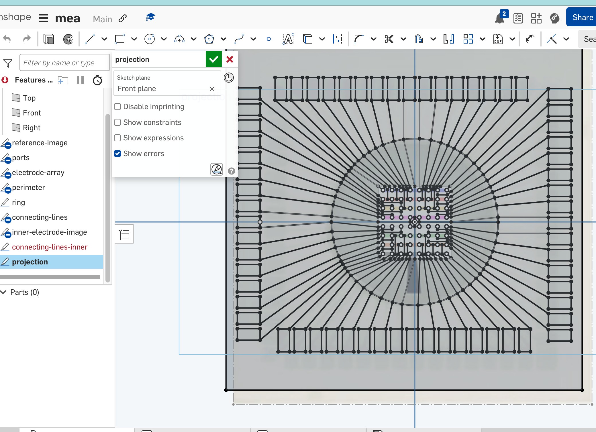
Iteration 1: OnShape.
Created at ~12 am from circles and linear patterns. I found out this shortcircuited, since I naively traced the well as a ring, so I created version 2!
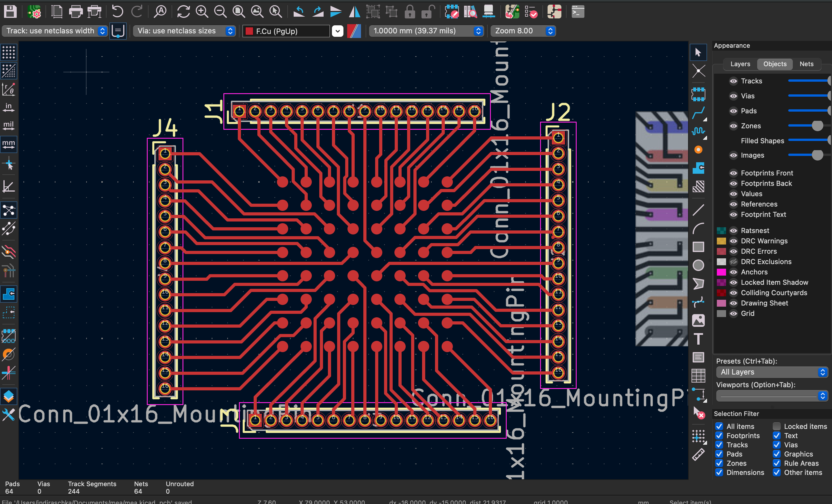
Iteration 2. The improved MEA in KiCad.
This dotted grid directly come into contact with neurons, and extend out to the peripherals.
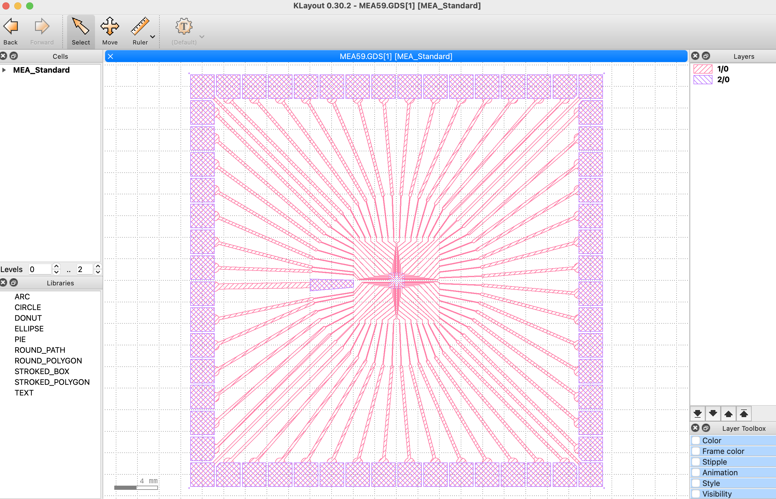
Iteration 3. Using existing MEA design files provided by Mind-in-Vitro, openable in Klayout.
3.4Most promising: Laser-induced graphene
3.4Most promising: Laser-induced graphene
At atopile's machine shop, we directed a laser beam at the polyimide tape, for graphene to become deposited on the surface. We are using microscope slides from frontier tower's biopunk lab run by Elliot Roth. Techniques were adapted from this porous graphene paper
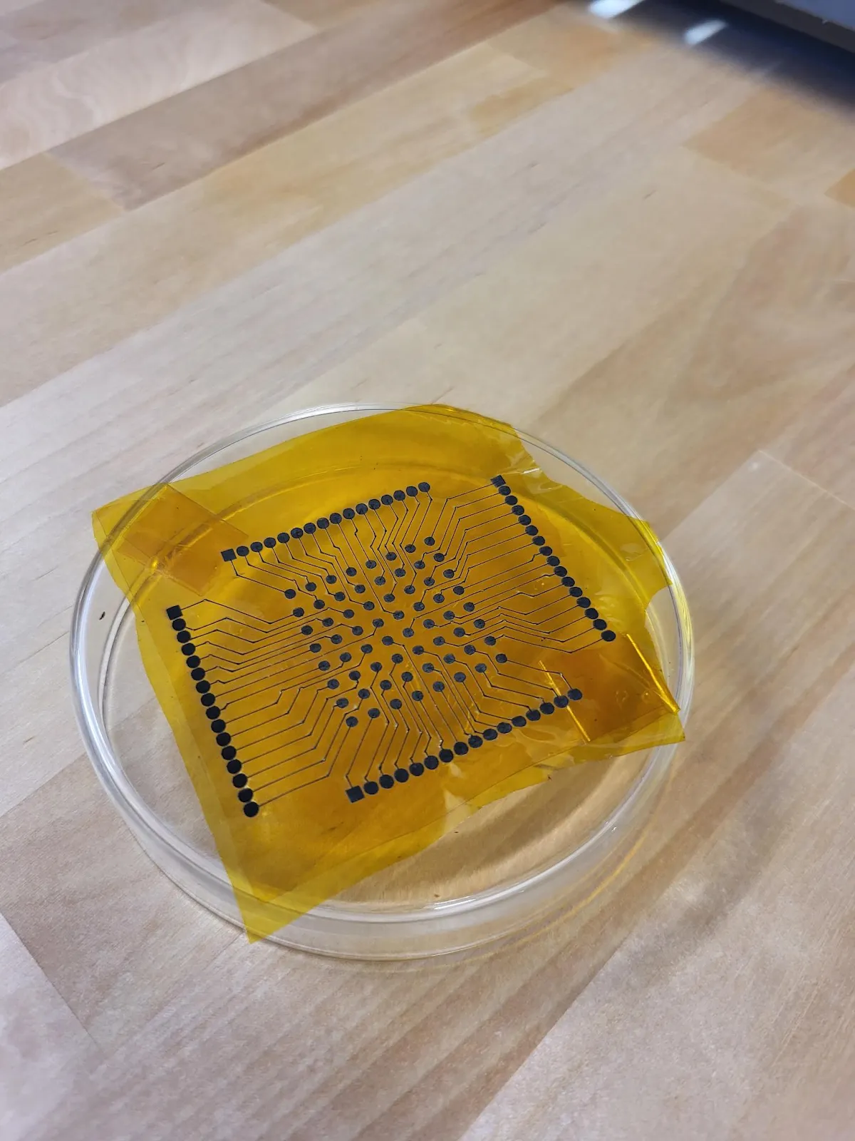
The laser’s energy causes lattice vibrations within the polyimide: Under high surface temperatures of >2 500 °C, C=O, C–N, and C–O bonds are broken, freeing non-carbon gases from this tape. The carbon atoms rearrange into graphene with its hexagonal structure.
We tuned a CO2 laser operating at 10 600 nm to 5.5W with a scanning rate of 88 mm/s with 100 lines/cm and directed the beam at the kapton tape.
The centre-to-centre distance between electrodes: 0.15 cm, with a 0.25 cm electrode radius. The trace width: 0.2 mm.
A hurdle is creating continuously conducting traces.
Trace width microadjustments
Given that SVGs are a set of lines defined using the XML format, we just made them thicker. However, in practice, laser software, e.g. Xtool or Lightburn, treat all lines as infinitely thin.
We then tried blowing up the JPGs, which are bitmaps; However, a change from 0.2 mm to 0.3 mm in the JPG led to a fuzzy visual appearance and shortcircuited. A lazy hack we found was just to duplicating the traces three times in the laser software from Xtool. Additionally, we varied the scan rate (+/- 20 mm/s) and lines per cm (max at 200, min at 50) and set the laser scanning to be monodirectional.
Examining raw trail conductivity
The triple-layered electrode version was consistently conductive. However, the graphene easily wears off, or encounters insulation at corners.
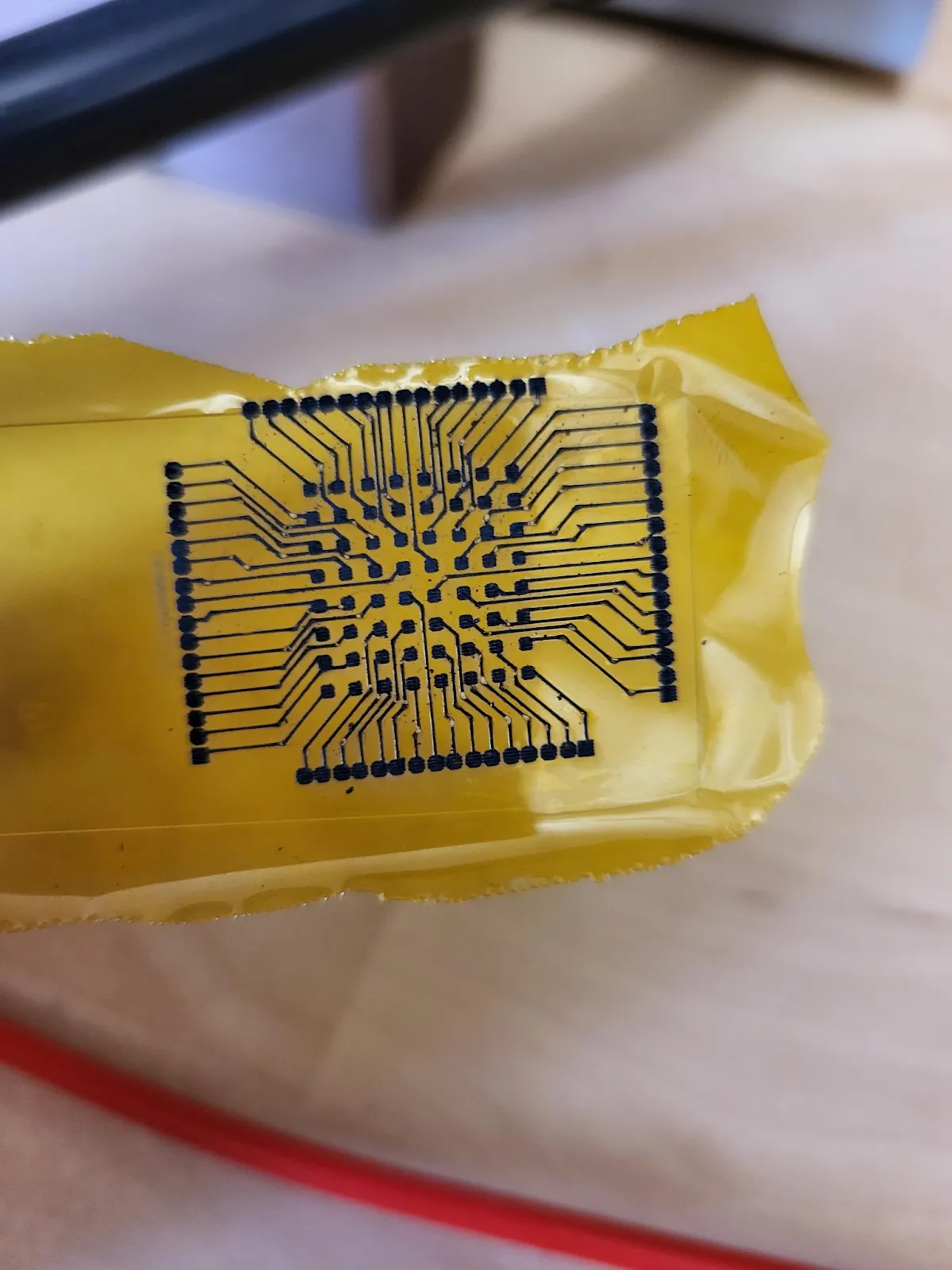
The next step would be more functional testing (saline) and compare to the standard Utah array.
3.52. Accidental discovery: Aluminum vapour deposition
3.52. Accidental discovery: Aluminum vapour deposition
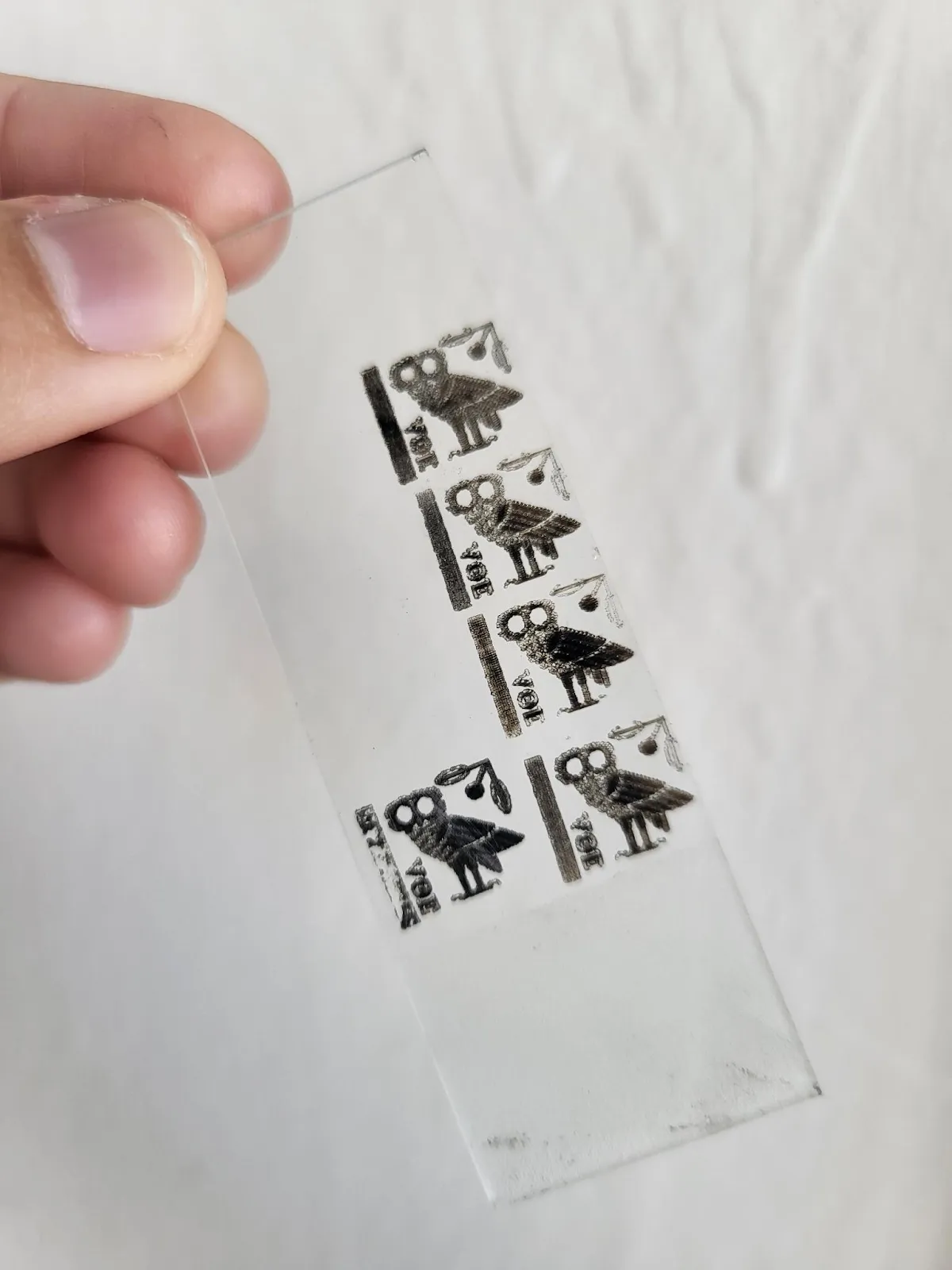
While implementing laser-induced graphene, we noticed dense metallic stripes appeared on glass--This certainly didn’t look like graphene. So we peeled off the kapton tape, put the glass slide into the laser chamber and turned the laser on again. This was in fact, the vapour from the underlying sheet of aluminum which had been sitting inside the glass in a diode-pumped solid state laser (DPSS) of 1064 nm (physical vapour deposition).
3.63. Error-prone: Copper metalization.
3.63. Error-prone: Copper metalization.
Review: In the traditional electroplating process, an object, the cathode, becomes coated with a thin layer of metal.
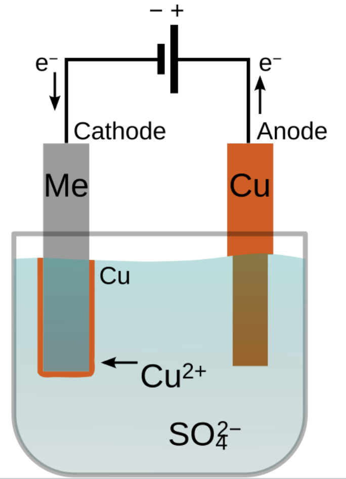
The cathode and the anode are initially submerged in ionic solution and a circuit is completed. When the battery applies its gradient, two processes happen:
- Chemical. The +ve ions start migrating to the cathode to coat it
- Electrical. The cathode "craves" electrons and the electrons move to the cathode. Simplified copper reaction: Cu²⁺ + 2 e⁻ → Cu(s).
In copper plating, a focused laser beam mimicks the voltage differential like a battery. As it is directed at the copper solution, it causes a thermal gradient: Heated and unheated surfaces. The heated area gains copper under the plate.
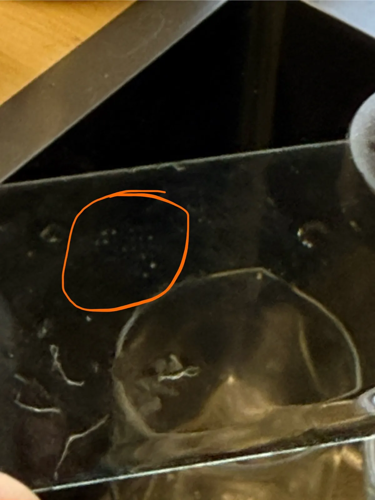
Results of the deposition
Preparing the electroplating solution
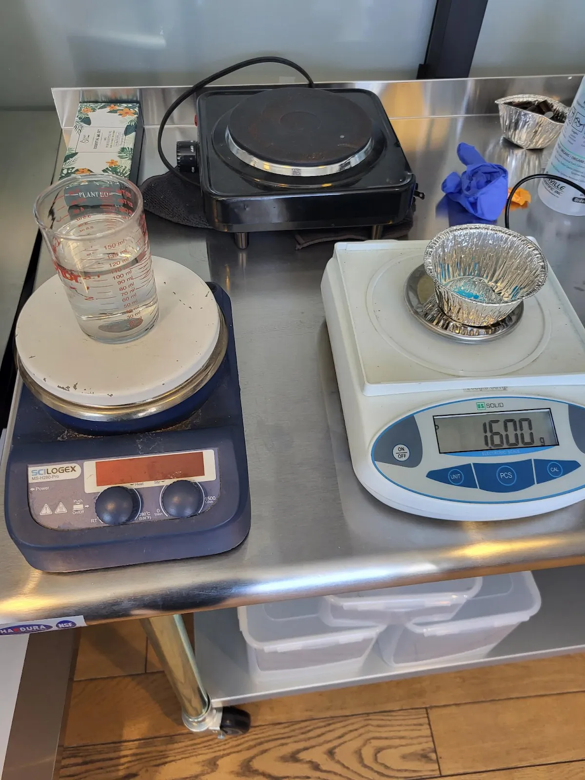
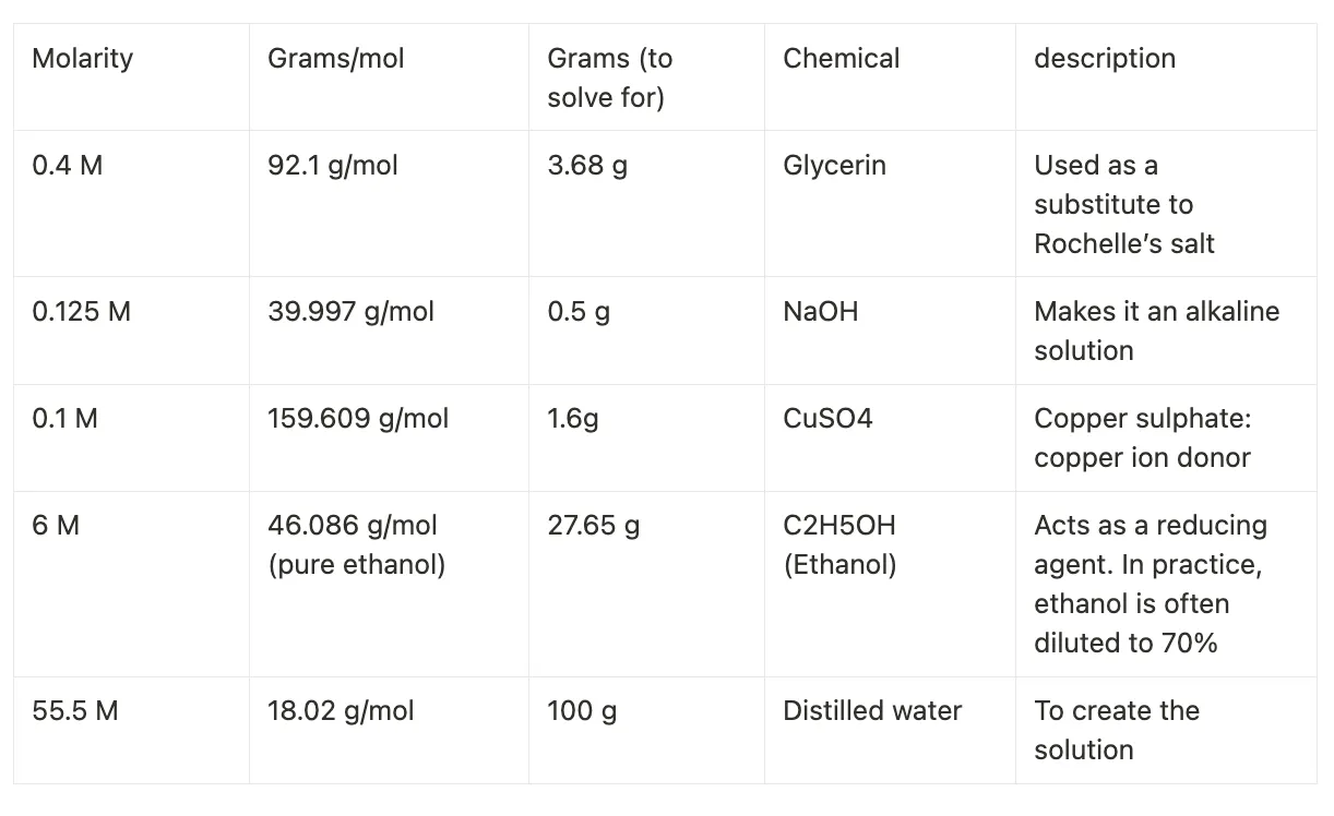
Add water first, and then add chemicals slowly from least reactive to most. i.e. Add distilled water, followed by alcohol, glycerin, NaOH and then CuSO4.
We placed the solvent on a hot plate, with a magnetic rod for stirring.
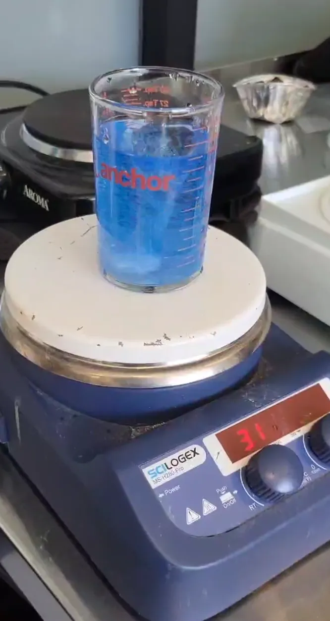
The biggest challenge here was when the scale started tweaking. We became suspicious when the 100 mL of water weighed 125 grams. Consequentially, in our 2nd copper replication attempt, the copper solution instantly precipitated into copper hydroxide--a cloudy, turquoise colour, not what we want! The ideal solution should look transparent, dark blue.
We tried a series of quick troubleshooting e.g. switching power supplies, using different scales, but there weren’t matching power supplies of 9V for any other scale in the lab.
Thus, I poured in some ethanol (1 mL of ethanol was 0.789 grams) to see how much the scale was off by--approximately 29.5875 grams. From then on, we performed everything according to the scale’s offset mass (1.25x). This method has been time-intensive and prone to error.
3.74. Not tested: PEDOT:PSS trails
3.74. Not tested: PEDOT:PSS trails
Motivation. Researchers may use red and green fluorescent proteins in their living neurons which includes filtering colours. So the yellow polyimide tape may present dark under a microscope. They have a perfect reason to want transparent MEAs?
Here are some materials to use (loosely inspired by this paper)
- Indium tin oxide coated borosilicate glass as substrate
- Brush-on negative insulator (1002F epoxy) - To cover the non-conductive regions
- PEDOT:PSS (PH1000 + 5 % DMSO or ethylene-glycol) - Making the surface biocompatible, although ITO is already safe.
Then, the plasma engine could increase the surface energy of glass.
3.8Next steps.
3.8Next steps.
It would be really good to replicate the entire neuronal headstage from Mind-in-Vitro to broaden the accessibility. Please get in touch corpus.logica@gmail.com if you want to support this project such as by offering ephys lab spaces.
3.9Credits:
3.9Credits:
Eigenlucy (main collaborator)
Supporters: Morgan Hough, Paul Han, Elliot Roth, Lucas Mair, James Mavo at frontier tower, San Francisco as well as Atopile for letting us use their office.
Funding: 1517 Medici project, merge grant, Lucas Chu and individual donors.
Highlight 4Assembling a microdrone [note-0033]
- 05-30-2024
- noesis
- #experimentalist-confetti
- #UAVs
Highlight 4Assembling a microdrone [note-0033]
- 05-30-2024
- noesis
- #experimentalist-confetti
- #UAVs
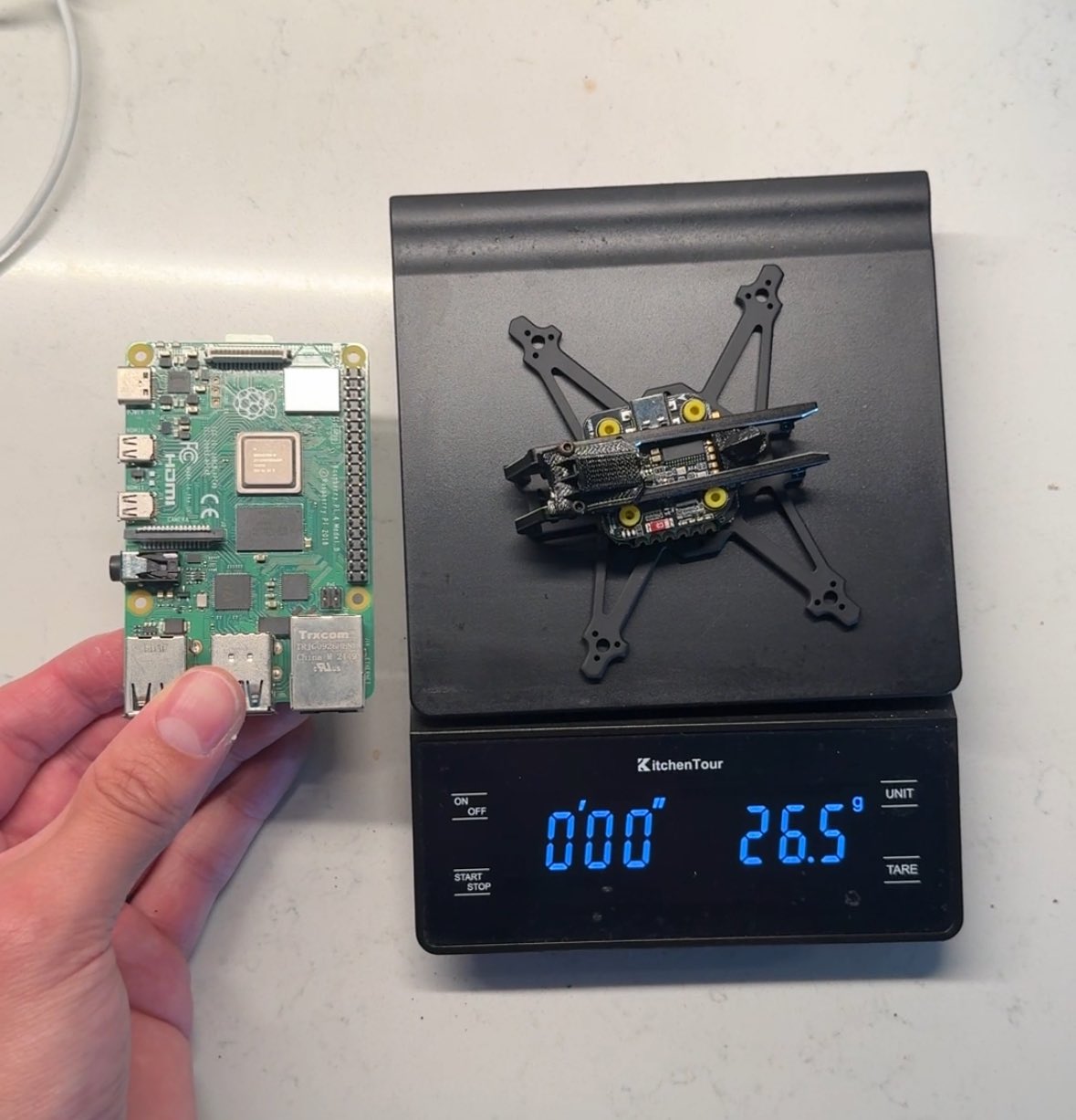
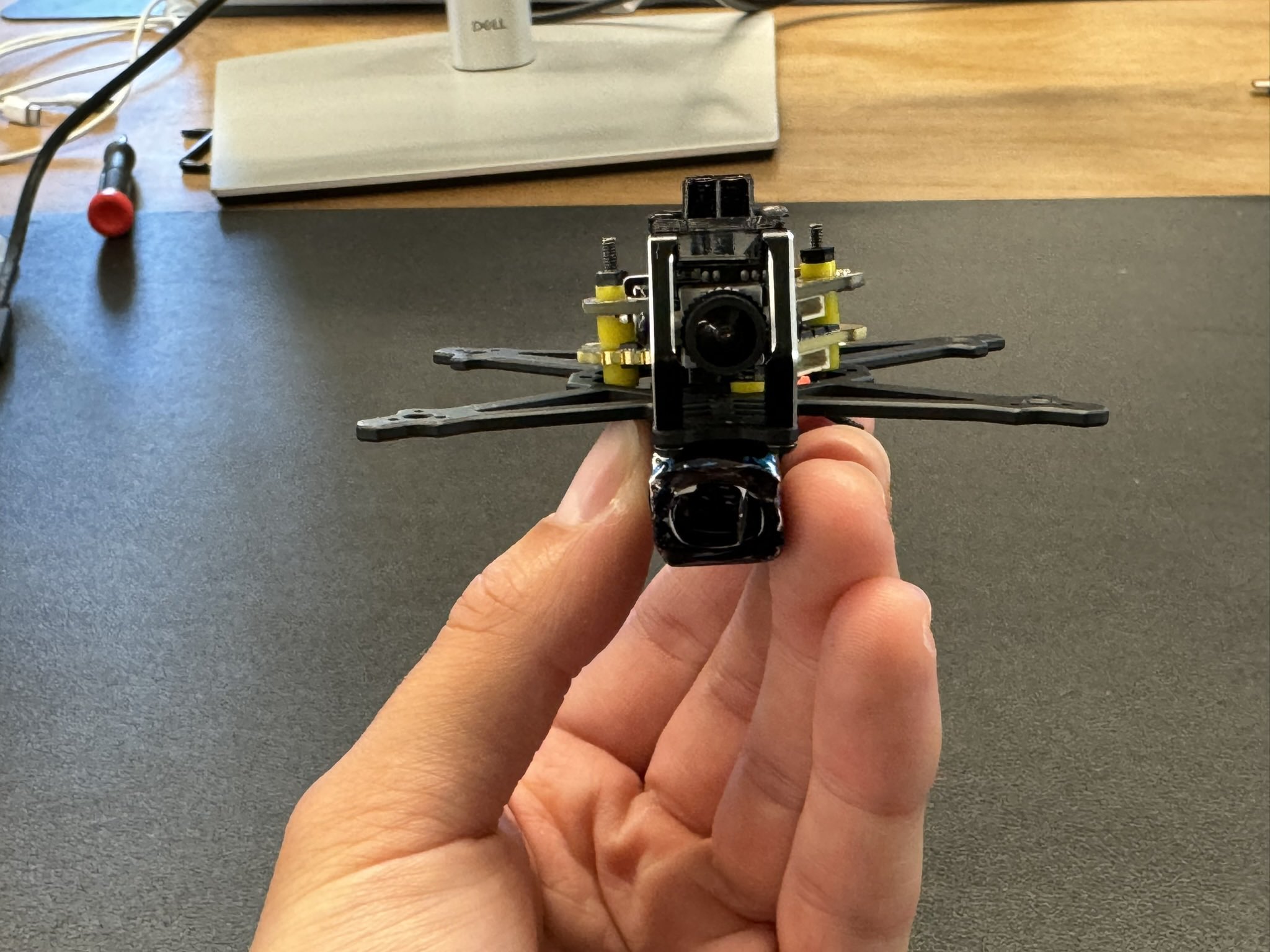
I met Chester at Founders Inc back then and then we worked on sourcing components andbuilding 1 - 2 microdrones, as well as simulating them in Unity.
Highlight 5Explaining Hikikomori in Japan [note-0020]
- 10-23-2023
- noesis
- #complex-systems
Highlight 5Explaining Hikikomori in Japan [note-0020]
- 10-23-2023
- noesis
- #complex-systems
Here is my essay for complex systems class at Minerva
A young man shut his door and didn’t come out for years. Mr. A was just a typical university student: He led a casual life and socialized with friends, holding part-time jobs on the side. However, he found himself in the same unstable job and aging past 30. Determined to find a permanent position, he quit his current job. However, after repeatedly unsuccessful attempts he withdrew completely, playing video games until midnight at home. After a quarrel, he cut off his brother and was financially supported by his mother. Mr. A also avoided any face-to-face contact (Kato et al., 2019).
Mr. A is an example of a ‘primary hikikomori’, accounting for 1.46 million in Japan as of 2023 (“1.5 Million People in Japan Living as Social Recluses, Many as a Result of the Pandemic,” 2023). 5 factors define a primary hikikomori according to trained Japanese clinicians:
- Spending most of their time at home for at least 6 months
- Persistent avoidance of social situations, including both work and school
- Significant distress associated with social isolation
- No apparent physical or mental etiology forcing the social withdrawal symptoms
- Be working age i.e. 15 - 64 years old (Suwa & Suzuki, 2013)
The definition of primary hikikomori is crucial for them to be recognized and receive help. This paper will explain the occurrence of primary hikikomori with the help of complex causality, system dynamics and network analysis lenses.
5.1Complex causality
5.1Complex causality
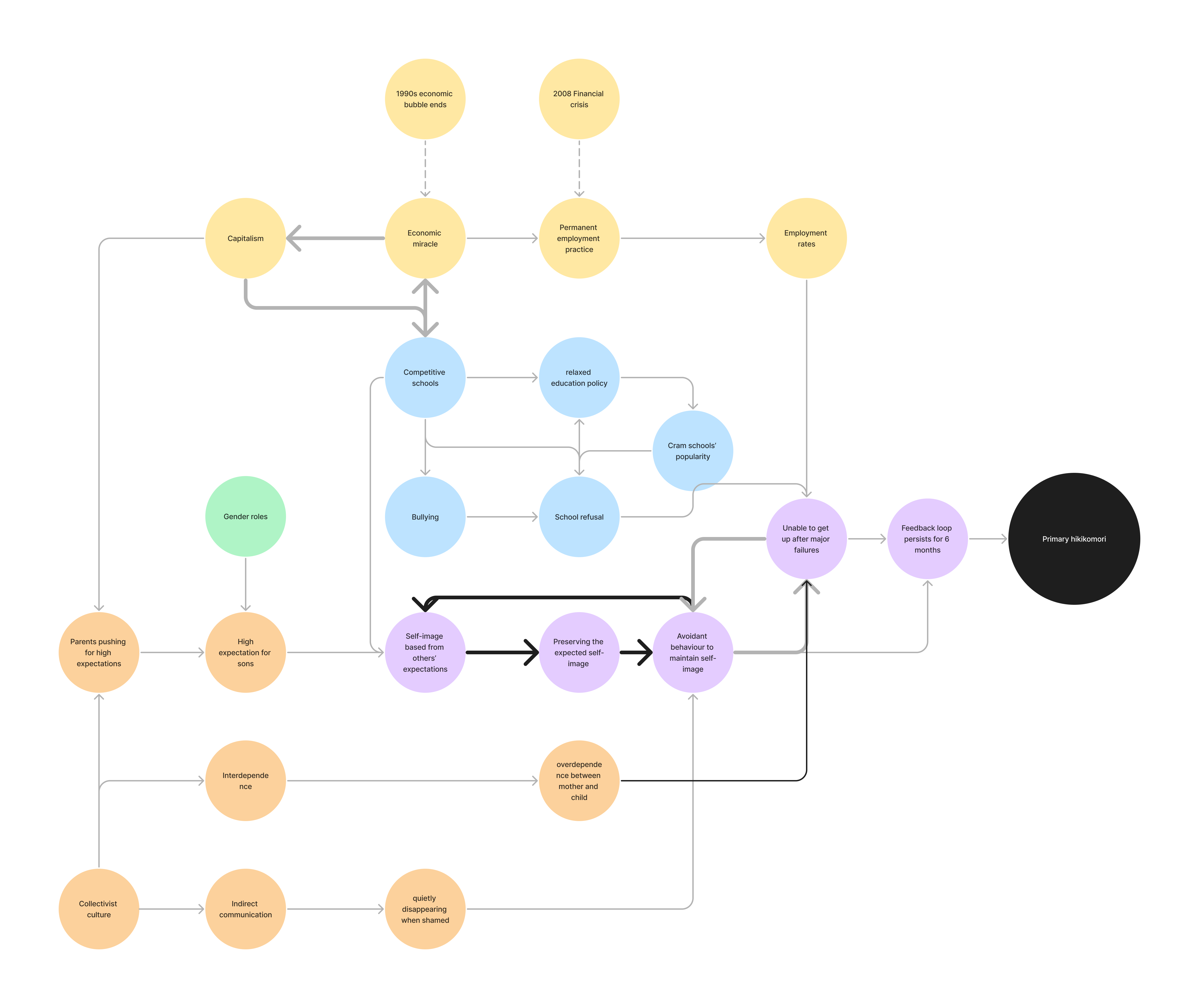 Fig. 1. Causal diagram for hikikomori.
Psychologically, hikikomoris base their self-image on others’ expectations. Others expect one to excel in examinations and jobs. Some individuals fall behind; Rather than getting up from major failures, they isolate themselves to avoid the negative judgement of others and protect their self-esteem. As isolation continues, the expected and the actual paths diverge even further. Individuals cling to the expected self in an attempt to protect their self-esteem, avoiding any behaviour—conversations, job interviews–that further damages it (Kato et al., 2019). Maintaining reputation is a reinforcing feedback loop that contributes to one becoming hikikomori. Avoidant behaviour and inability to get up after major failures are necessary factors which reinforce each other. When this feedback loop lasts for more than 6 months, it is necessary and sufficient to cause hikikomori behaviour. These psychological factors are shown by purple nodes in the causal diagram.
In Japan, school refusal started to become prevalent in the 1970s and 80s (Cerantola, 2019). On “17 October 2019, the government announced that absenteeism among elementary and junior high school students had hit a record high, with 164,528 children absent for 30 days or more during 2018” (Cerantola, 2019). School refusal can be a salient factor for entering into a reinforcing loop as mentioned above. Anthropologist Anne Allison suggests that after World War II, the Japanese education system became focused on “highly competitive and rigorous high-school testing…The goal was to prepare students for equally arduous employment in Japan’s industrial capitalist economy” (Berlatsky, 2013). Some students experience bullying, which is even termed “natural selection” by some parents. In 1998, in response to increased school refusal, the Japanese government proposed the relaxed-education policy, which intends to give younger generations less pressure. It was implemented for twenty years, however, as reflected by Japan’s decreasing rank on PISA exams since 2000, schools became inattentive to fundamentals (Zhou, 2017). As capitalism continues, it means that students also have to attend cram schools. Competition, control, bullying and relaxed-education policy are four salient factors for school refusal, shown in blue in the causal diagram.
From the 1920s to the Japan post-war economic boom, it was easy for men to get a permanent position at a big company to support a family (Dwyer, 2009). The collapse of the bubble during the 1990s brought instability, uninviting work conditions and unemployment (Kato et al., 2019). After the 2008 financial crisis, many Japanese companies discontinued the permanent employment practice, causing job insecurity (Dwyer, 2009). Economic factors were displayed using yellow nodes.
Japan is a collectivist culture where common goals are emphasized above individual needs, leading to three main implications. Firstly, people are valued if they support the goals of others, forming an interdependent society. Dependence is an acceptable mode of behaviour in Japan even in adult life. For example, as part of the heightened industrialization in the 1980s, employees are encouraged to view their companies and colleagues as part of an extended family, forming close ties (Kato et al., 2019). Interdependence can become parent-child overdependence where the child resorts to parental support after failure. Next, parents have much determination in their child’s goals and high expectations fueled by capitalism. Note that interdependence and parental expectations don’t necessarily conflict with each other: It’s common for therapists to hear parents speak proudly about their hikikomori child’s excellence, believing they can still achieve something in the future while continuing to financially support unemployed children. There is a gender stereotype for men to be strong across cultures. Japanese parents have high expectations for their sons to enter elite universities and land a job in top corporations, and parents are alarmed by the slightest deviation (Ma, 2016). Parents’ expectations tie into the child upholding self-image as aforementioned. Thirdly, in a collectivist culture, one also wants to be quiet about their own needs, giving rise to indirect communication. Particularly, "Making oneself disappear” in social situations where one is shamed has long been considered a virtue, fueling hikikomori’s avoidant behaviour (Kato et al, 2019). Therefore collectivism has three implications that intensify hikikomori behaviour. Psychological, workplace, educational, cultural and global causes spanning the multiple levels of analysis are all salient factors to the emergent property of primary hikikomori.
5.2System mapping
5.2System mapping
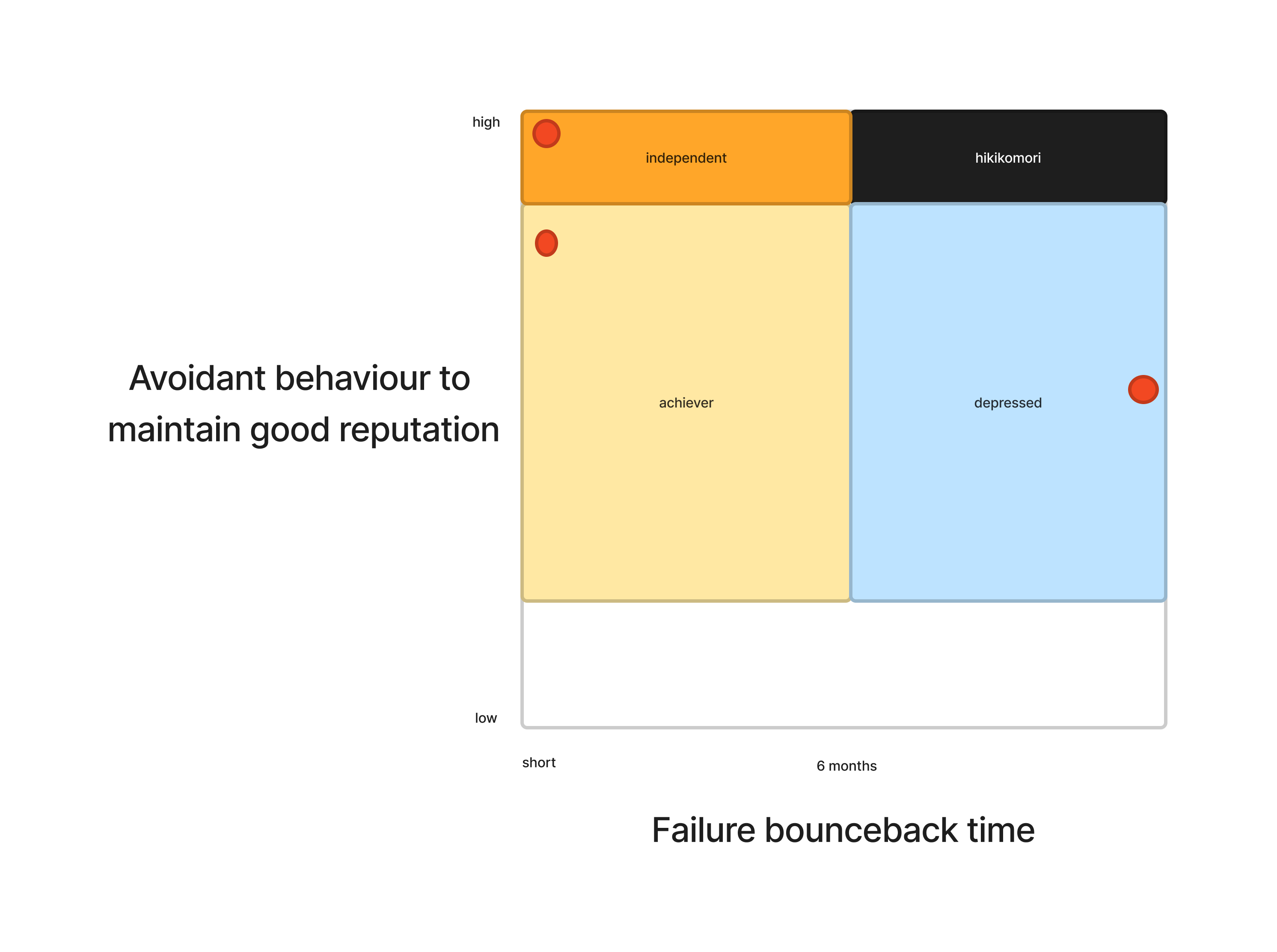 Fig. 2. A 2-dimensional phase space for individual’s achievement style
Two factors: Time needed to get up after major failures, amount of avoidant behaviour to maintain reputation and the duration of this reinforcing feedback loop can be used to estimate if an individual is hikikomori.
5.3System dynamics
5.3System dynamics
Similarly, from the same two factors, an achievement styles phase space can be constructed. The phase space contains 5 basins around their respective attractors. Firstly our causal diagram explains the attractor on the top right. However, if the failure bounceback time is less than 6 months and an individual is highly avoidant, they’re classified as an independent person. Next to the hikikomori is the depression basin. The characteristic hopelessness contributes to an attractor with a long bounceback time and moderate avoidant behaviour. Similarly, achievers are attracted to showing only their successes and strive to get up from failures extremely fast. Finally, we have a white space since many vastly different individuals have low avoidant behaviour and their trajectory is unpredictable.
External forces can cause a regime shift. Kenta became a hikikomori after being ostracized at school for his high-pitched voice. A young woman known as a “rental sister” began sliding letters under his door, gradually inviting him to walk in nature, exercise and eat out, helping to reduce his avoidance. She supported his self-esteem, reducing the failure bounceback time. Kenta still lives on his parents’ money but has moved out (BBC News, 2019).
Rental sisters can help hikikomori break the bifactor feedback loop. They are a type of home-visit service offered by the non-profit organization ‘Newstart’. Later, hikikomoris will transition to a program to live together with other hikikomori, work as a team in restaurants and bakeries and receive employment seminars (Ismail, 2020).
Yuto became hikikomori after burnout at the end of high school. After being helped by Newstart for a year, he was studying for his driver’s license, attending school to become a graphic designer. He maintains a good relationship with his parents. Now, he lands in the white space on the phase diagram (Ismail, 2020). As of 2021, “New Start has helped around 3,000 Hikikomori go back to regular life” and about 80% of clients successfully reestablished themselves (BBC News, 2019). Network
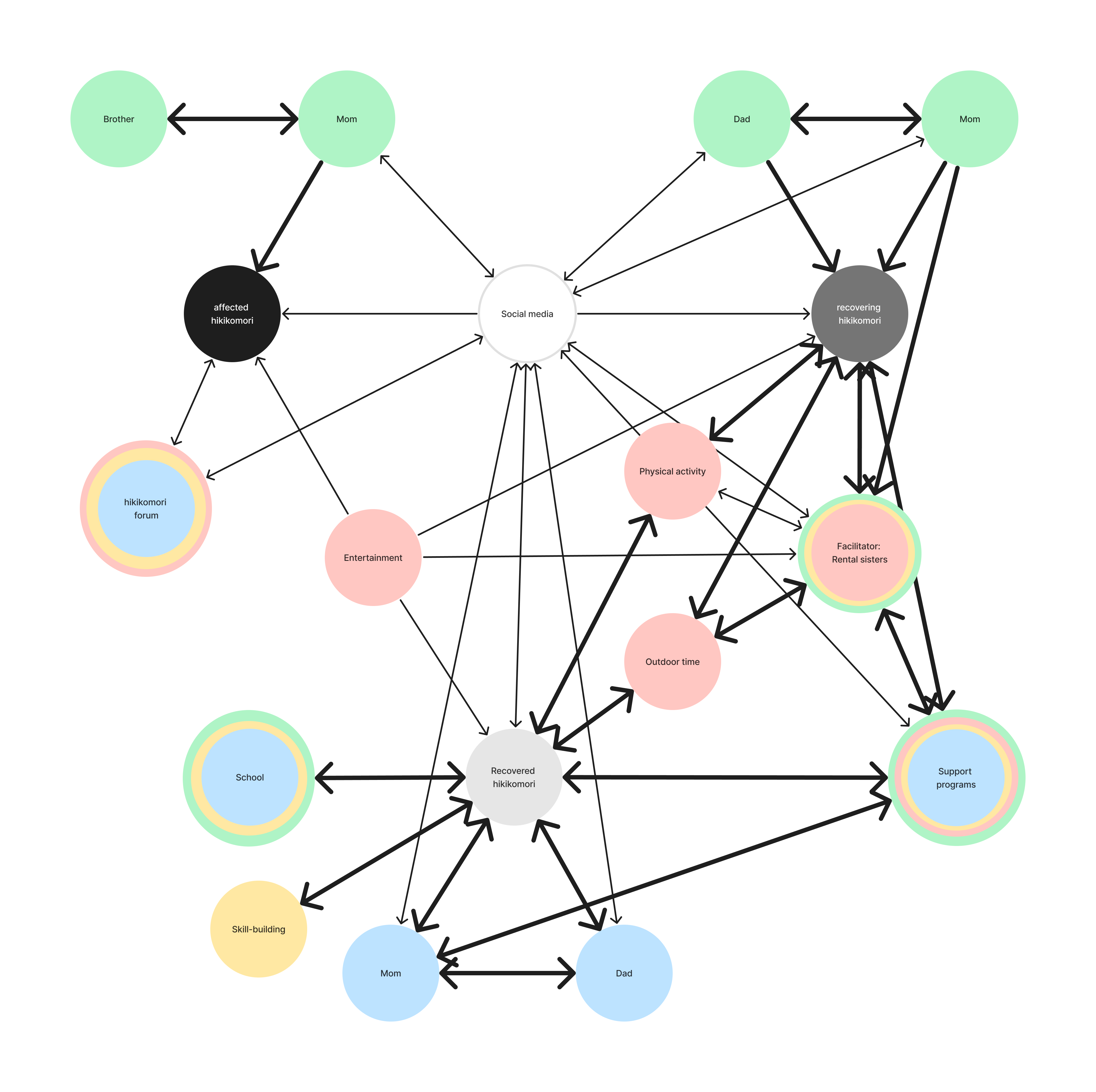 Figure 3. A network diagram based on three hikikomoris at different stages of recovery.
Based on the case studies for hikikomoris at different stages of recovery, a sample network consisting of the individual and their respective activities were created. In the network, each node is a source of activity, such as Mom or entertainment. Since humans need all four types of support relationships, each activity is classified by its support role to the closest hikikomori: Emotional (red) refers to an activity which brings physical or emotional comfort. Esteem (yellow) means an activity which reminds one of their strengths. Informational (blue) refers to informative activities which suggest the next steps. Tangible (green) relates to offering resources for someone to solve a problem (Scott, 2023).
Each edge represents an exchange of information between two entities, with direction representing where information flows. A weighted edge represents an offline interaction while an unweighted edge represents purely online interactions.
The affected hikikomori (Mr. A) has a degree of 4: An in-degree of 4 and an out-degree of 1. He consumes entertainment sources, social media and hikikomori forums as well as gets tangible support from Mom. However, he only communicates in online forums. The surrounding network is not robust with only one source of each kind. For example, if the node 'online forum' is removed, the hikikomori will have trouble finding esteem support and may further avoid in-person communication. In the case of a recovering hikikomori (Kenta), degree centrality increases–The degree of the node is 8: 8 in-degrees and 4 out-degrees. The number of weighted edges increases. The surrounding network becomes more robust as more sources of emotional, tangible and esteem are present. However, parents are still offering monodirectional financial support.
For a recovered hikikomori (Yuto), the degree of the node is 9: 9 in-degrees and 8 out-degrees. The degree is even higher compared to the recovering individual. A key difference is parents became informative support nodes with bidirectional communication. Secondly, there are even more sources for each type of support.
In general, as a hikikomori recovers, the degree centrality, weighted edges and surrounding robustness for multiple sources increase. The network exhibits a small world effect: Hikikomori all receive information from online sources. Parents can use social media to contact support programs with a geodesic distance of 2 to reach any hikikomori. Aside from Newstart, corrective solutions include virtual AI companions like character.ai, and physical robots like “OriHime” while affirmative solutions include free schools and metaverse social events (Montgomery, 2021). Shut-in behaviour is also occurring outside Japan; In South Korea, 660 000 people between the ages of 20 and 39 live the equivalent life. Having given up on exams, work, raising children and N number of things, they are labelled as the “N-po generation” (Liu, 2023). In China, the Lying Flat movement which gained popularity within the last 5 years is a close analogy, featuring youths figuring out how to live the lowest stress life at the lowest cost. The collective isolation behaviour been reported in other countries such as India, Brazil, the United States, Iran, Australia and more.
Hikikomori is a problem which is difficult to understand linearly. Rather than a singular cause, a complex causality lens suggested that most factors across levels of analysis are salient and identified feedback loops that solutions can target. Similarly, the system dynamics lens highlighted plausible solutions that shift the regime into adjacent basins. Finally, network analysis showed relationship trends for recovering hikikomori. These insights from a complex systems perspective can act as important constraints to guide future solutions to a global problem.
AI statement: Grammarly was used for sentence-level editing.
5.4References
5.4References
- BBC News. (2019). Rent-a-sister: Coaxing Japan’s hikikomori men out of their bedrooms. YouTube. https://www.youtube.com/watch?v=q9IRmUEsz6g
- Berlatsky, N. (2013, November 22). Japan's Cutthroat School System: A Cautionary Tale for the U.S. The Atlantic. https://www.theatlantic.com/education/archive/2013/11/japans-cutthroat-school-system-a-cautionary-tale-for-the-us/281612/
- Cerantola, A. (2019, December 23). Why so many Japanese children refuse to go to school. BBC. https://www.bbc.com/news/world-asia-50693777
- Dwyer, J. (2009, January 25). Japan’s ‘employment for life’ myth. The Institution of Engineering and Techology. https://web.archive.org/web/20100506074824/http://kn.theiet.org/comment/management/Dwyer-comment-69.cfm
- Ismail R. New starts at New Start: Recovery and the work of hikikomori. Transcultural Psychiatry. 2020;57(5):698-709. doi:10.1177/1363461520958337
- Kato, T.A., Kanba, S. and Teo, A.R. (2019), Hikikomori : Multidimensional understanding, assessment, and future international perspectives. Psychiatry Clin. Neurosci., 73: 427-440.
- Liu, Z. (2023, June 30). Hikikomori, N-po and lying flat - Snapping in East Asia. Erasmus Universiteit Rotterdam. https://www.eur.nl/en/news/hikikomori-n-po-and-lying-flat-snapping-east-asia
- Ma, K. (2016). Why are there gender differences in hikikomori? Quora. Retrieved October 26, 2023, from https://www.quora.com/Why-are-there-gender-differences-in-hikikomori
- Montgomery, H. (2021, November 29). Japan Has an 'Alter Ego' Robot So You Can Go Out Without Going Out. VICE. https://www.vice.com/en/article/93bbaz/japan-robot-hikikomori
- 1.5 million people in Japan living as social recluses, many as a result of the pandemic. (2023, April 1). The Japan Times. https://www.japantimes.co.jp/news/2023/04/01/national/hikikomori-numbers-pandemic/
- Scott, E. (2023, September 18). Types of Support: How Does Social Support Work? Verywell Mind. Retrieved October 26, 2023, from https://www.verywellmind.com/types-of-social-support-3144960
- Suwa, M., & Suzuki, K. (2013). The phenomenon of “hikikomori” (social withdrawal) and the socio-cultural situation in Japan today. Official Journal of the Italian Society of Psychopathology, 19, 191-198. Zhou, J. (2017). How Yutori Kyoiku Affected Japanese Students’ Learning Abilities [Panel Presentation]. https://mds.marshall.edu/colaconf/2017/day1/8/
Highlight 6Mapping haptic gestures to swarm robots [note-0056]
- 06-20-2023
- Sean Wang, noesis
- #swarm-algorithms
- #robotics
- #haptics
- #ml
Highlight 6Mapping haptic gestures to swarm robots [note-0056]
- 06-20-2023
- Sean Wang, noesis
- #swarm-algorithms
- #robotics
- #haptics
- #ml
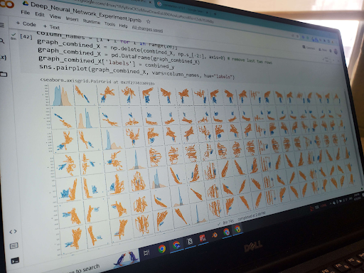
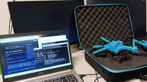
At UWaterloo ERABLab, we built a neural network that recognizes gestures of the Senseglove haptic hand and controls the motion of brushbots with Professor Gennaro Notomista. This involved learning linear algebra, some multivariable calculus, neural networks, the PyTorch framework, Linux and ROS. There was a more-than-expected amount of troubleshooting.
Highlight 7Neuralink: neuroscience, engineering and prospects [note-0035]
- 01-04-2022
- noesis
- #neuroscience
- #engineering
- #invasive-BCIs
Highlight 7Neuralink: neuroscience, engineering and prospects [note-0035]
- 01-04-2022
- noesis
- #neuroscience
- #engineering
- #invasive-BCIs
A powerful AI is sending your family to Andromeda. You wail loudly, but even so, only at 130 words per minute. You type on a keyboard and even try handwriting in desperation. However, the AI thinks you’re too incompetent and continues regardless. The speed of communication will limit a species’ performance — the ability to learn, work, create, have empathy for each other and everything else we do. To tackle this barrier, a slighly controversial company Neuralink has emerged. The company develops implantable Brain-Computer Interfaces (BCIs) and was founded by Elon Musk and others in 2016. We’ll dive into how the device works and if neuroscientists think the company is legit. Then, we’ll paint how similar BCIs impact human learning, work, creativity, and health. Finally, a few steps to make related research fruitful.
7.1This article will discuss
7.1This article will discuss
Background
- The fundamental unit of the brain
- What are Brain-Computer Interfaces?
Neuralink
- Neuralink’s near term goal
- How the link reads & writes to the brain
- Pig demonstration
- Monkey demonstration
- Perspectives on Neuralink
Applications of BCIs
- Redesigning learning & notetaking
- Smart workplaces
- Everyone can be an artist
- Quality sleep
The future
- How to advance the field of BCIs
7.2This article will not discuss:
7.2This article will not discuss:
- The ethics of BCIs
- The metaphysics of intelligence and intelligence amplification
7.3Background
7.3Background
Before we learn about Neuralink, let’s look very briefly at how the brain works.
This is a single neuron, the fundamental unit of the brain.
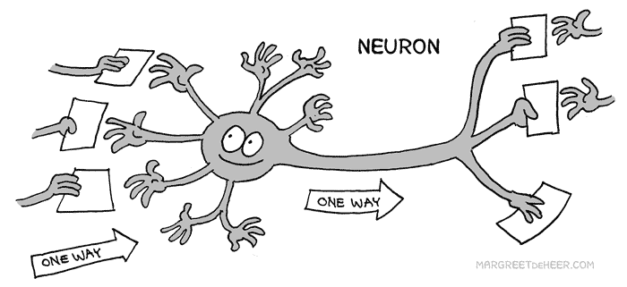
Essentially, a neuron receives inputs, computes and decides to pass on or abandon a message. The input comes in the form of neurotransmitters, e.g. Dopamine, serotonin, at the dendrites.
Then enter the computation phase. The number being modified is called the resting membrane potential.
As a neuron is in a soup of ions (charged atoms) and the interior of the neuron is more negatively charged than the outside. This causes a voltage difference or a resting membrane potential of -70 mV. A number of ions, such as K+, Cl-, Na+ flow in and out of the neuron membrane. Example ions include: As there is a negative charge inside the neuron, Na+ ions flow into the neuron. The membrane potential begins to increase from -70 mV. If it goes above -55 mV, then an electrical current is generated and sent down the axon. This is called the action potential, spike, impulse, or firing of the neuron. If the neuron doesn’t match the threshold, then nothing happens.
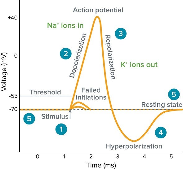
As the neuron is now positively charged, K+ ions travel out of the membrane for the neuron to return to its resting potential. Meanwhile, the electrical message has travelled to the end of the axon (see diagram). A way to continue the message is to release neurotransmitters across the synapse into the dendrites of the next neuron. The next neuron then “computes, passes or abandons” accordingly.
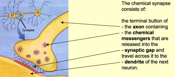
Our “input, compute, pass or abandon” is a vastly simplified model, not to mention from a computational standpoint. In the real brain, neurons are more like tangled yarn. Large numbers of them are connected in series and parallel, the signals converge and diverge, as an example, a typical cortical neuron has 1000–5000 synapses.
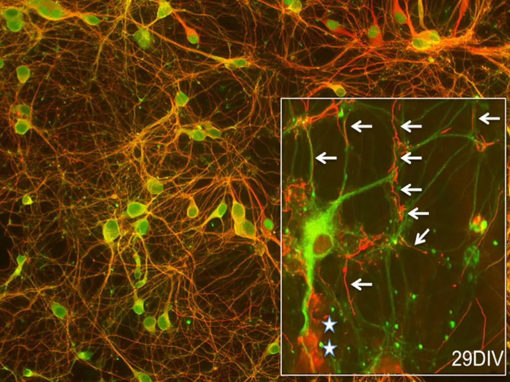 Example: Rat cortical neurons.
Plus, neurons can fire 100 times per second.
7.4What is a Brain-Computer Interface
7.4What is a Brain-Computer Interface
To read the complicated organ, our device must be able to detect the location of the spikes, from a larger number of neurons and reflect neural changes quick enough.
These requirements are known as, high spatial resolution, scale and temporal resolution.
The device which reads the brain is a kind of a Brain-Computer Interface (BCI), sometimes called a Brain-Machine Interface (BMI).
An example of a BCI. It decodes mental handwriting.
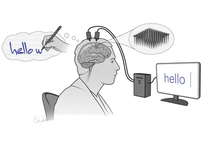
BCIs could also be used to stimulate the brain. What is Neuralink Neuralink is making a BCI which is implanted in the scalp. Its near-term purpose is to solve brain and spine problems. Namely, the company mentioned depression, anxiety, insomnia, memory loss, hearing loss, blindness, kinds of paralysis, paraplegia, etc. Presently, patients with neurodegenerative diseases require risky surgeries:
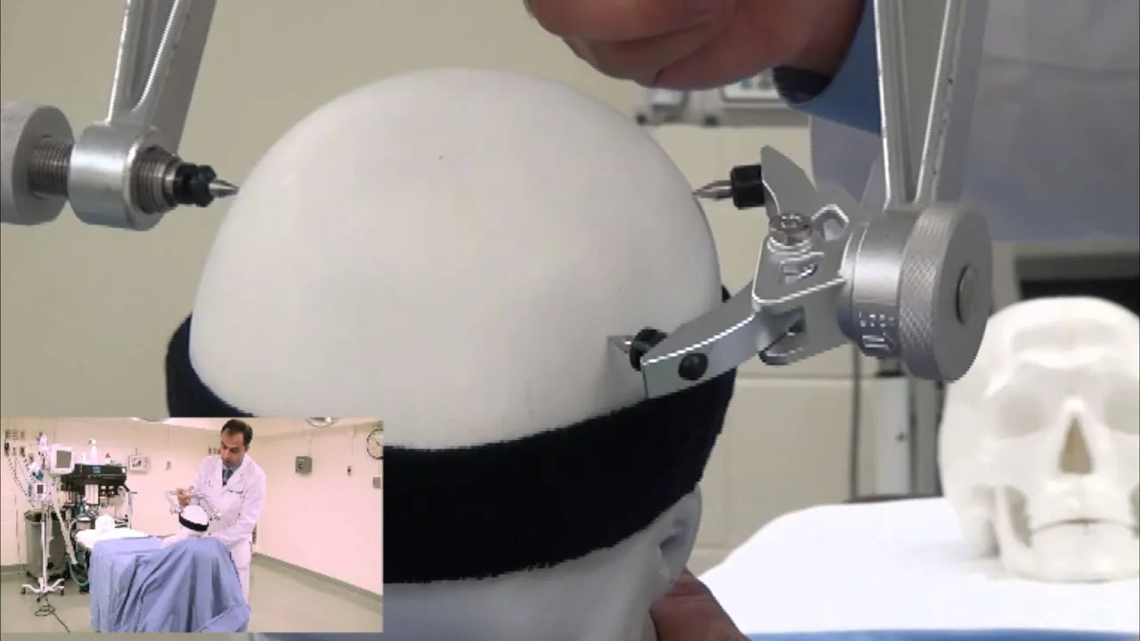
7 possible risks of neurosurgery
- The patient’s hair must be shaved prior
- Wide opening on the scalp, possibility of scar formations
- General anesthesia side effects
- Surgeon errors
- High cost
- The need for more surgery
- Scarring the brain
Some BCIs are already used to partially replace neurosurgery, e.g. deep brain stimulation, where the device can send electrical impulses to stop an incoming seizure. However rigid metal probes can cause foreign body responses from the brain, causing scars that eventually deteriorate signals.
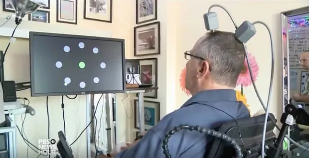
The Utah Array
Often, large boxes, which contain algorithms and batteries, come out of the head, meaning more risk of infection. The device also requires experts to follow around the patient to use. Meanwhile, Neuralink is about the size of a small coin (23mm diameter, 8mm tall). It aims to influence a large volume of neurons while being as easy and fast to install as LASIK. it is barely visible after the implant.
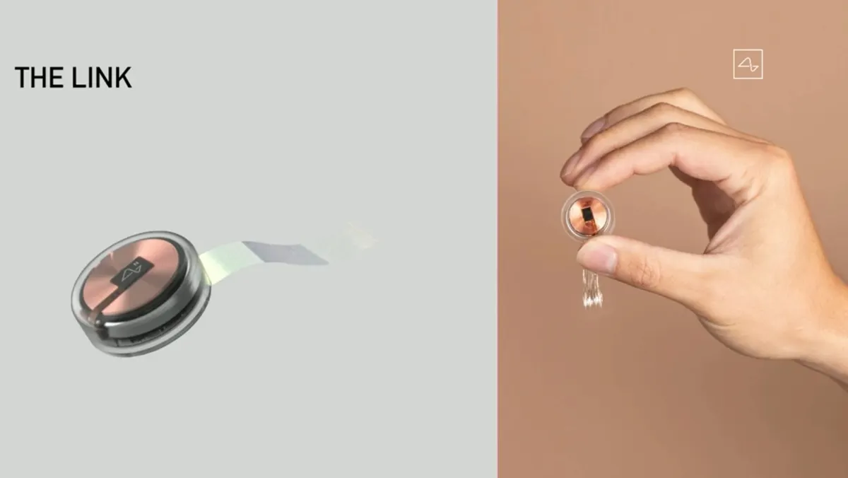 The Neuralink chip, the Link, with extending electrodes
How Neuralink works
The chip has a total of 1024 electrodes, each able to record/stimulate between 1000 to 10000 neurons. This gives control over a total of 10 million neurons. Every 16 electrodes belong to one thread, with 64 threads in total and spaced out by 200 microns. As each electrode is below visible length and should be placed 60 microns near a neuron, a robot is employed for the surgery. An opening the size of Neuralink will be created in the skull, covered by the module and the process will only require partial anesthesia.
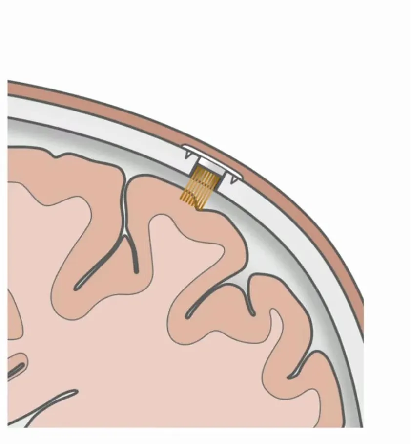
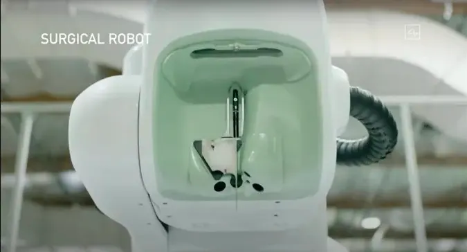 The robot can sew electrodes while dodging veins, arteries at a maximum rate of 192 electrodes per min.
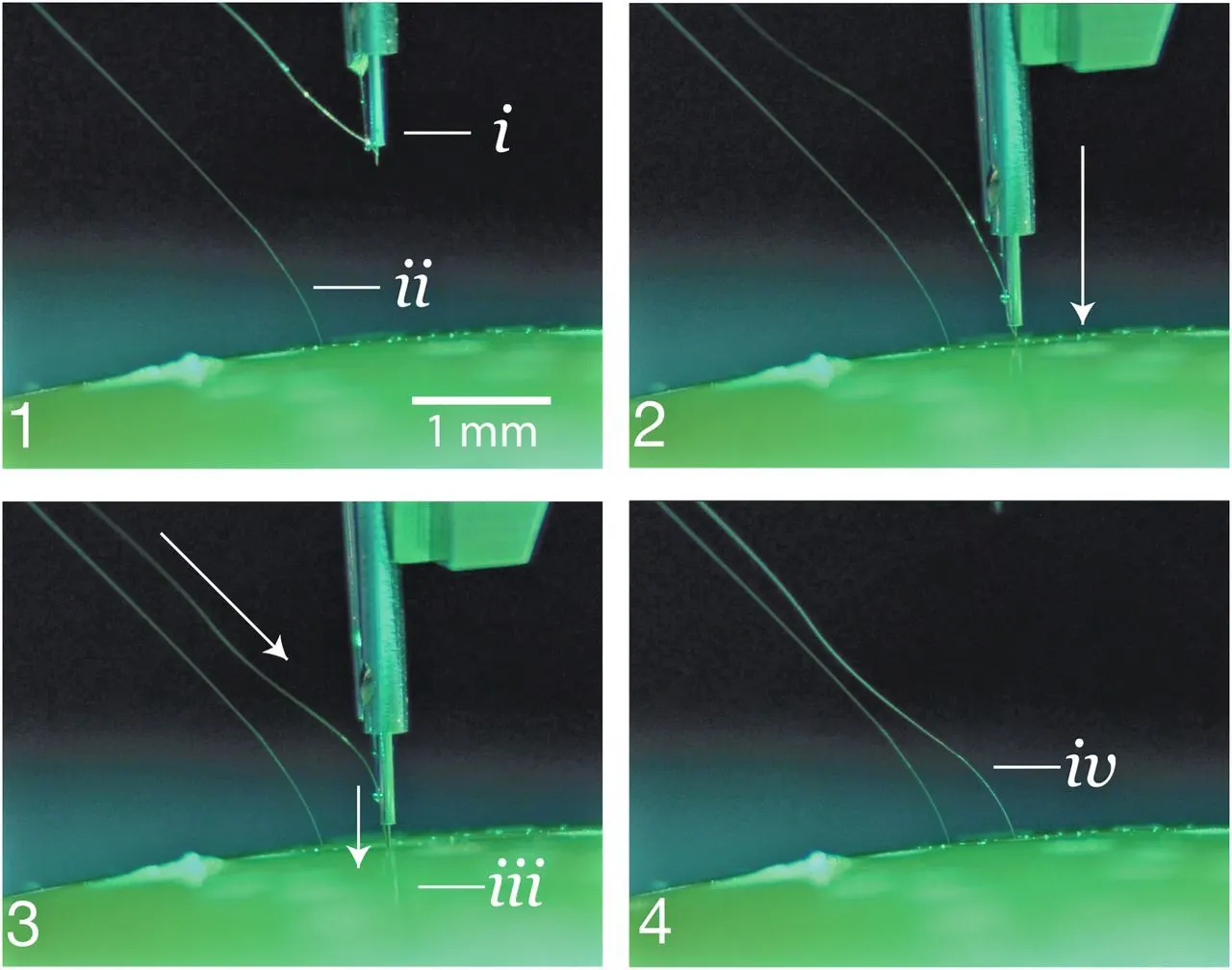
The needle pincher cartridge of the robot implanting the electrode
Here is the process of reading the brain:
Neuron spikes → picked up by probes → signal processed on-chip → signal transmission → computer/phone responds When there is a voltage change in neurons, an electric field is produced. An electric current passes through the electrode. This is a flexible electrode made by a biocompatible material, polyimide, wrapped around gold.
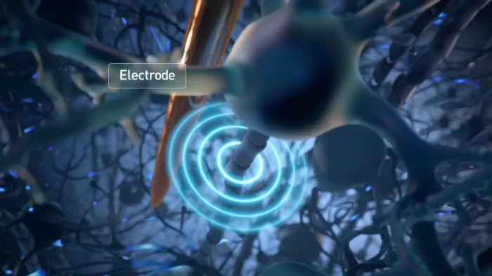
Each of the 1024 electrodes amplifies electrical activity, filters noise and digitizes the spikes.
From this:
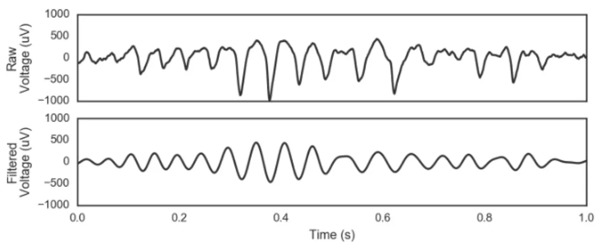
To this:
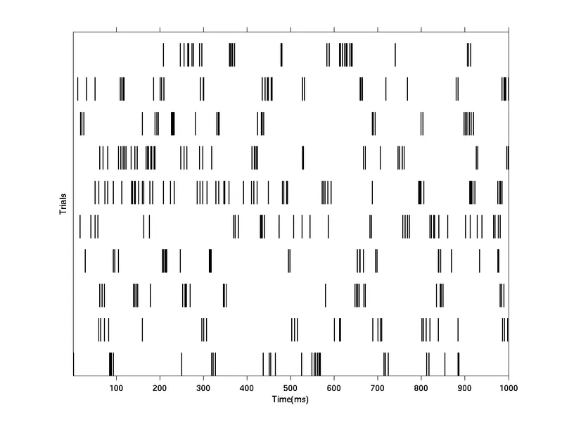
As all 1024 electrodes are simultaneously monitoring electrical activity, there is a huge volume of data to be processed. Sending them to a computer would delay the BCI. If a user wants to catch a ball, the BCI has to decode the intent in split seconds which then enables the user to do something else. The set of instant interactions is referred to as a closed-loop system.
Thus, all 64 threads (each containing 16 electrodes) connect to the custom ASIC that contain algorithms, spike detection, battery, communication processes, etc. There are four 256-channel chips within the ASIC.
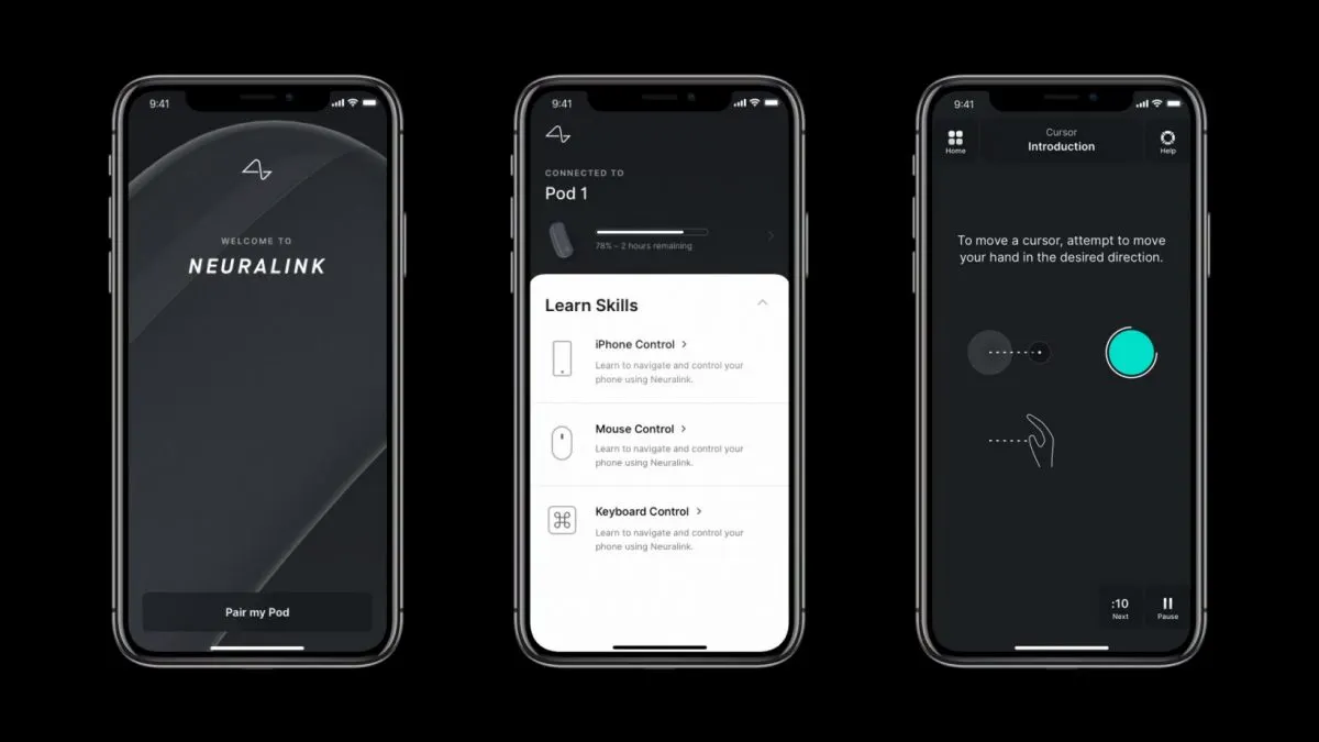
On the ASIC, machine learning algorithms detect spikes and assign them to neurons. Spikes are detected in 25 ms windows, or bins with the spike count represented by a 4-bit number. In total, there is 4041024 = 20 kB of information per second. Along with the number of spikes, there are extra bits of information about the width, height of the spike etc. Information is transmitted via Bluetooth to a smartphone app with controlling software.
Writing
Each electrode can release current to flow along the neuron, causing a chain of spikes. Current can be as low as 10 microamps as far as 4 mm away.
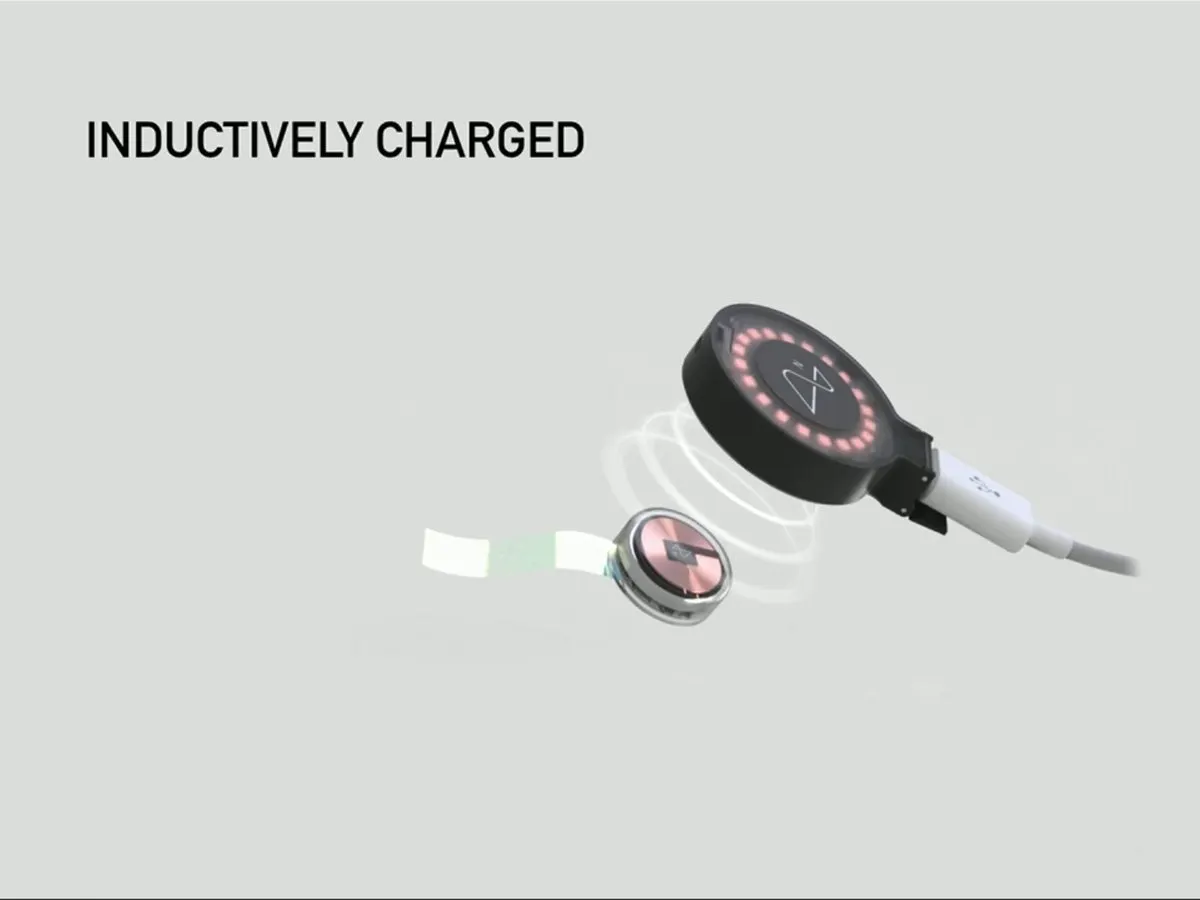
Charging
An implanted link can last around 12 hours and can be charged inductively.
This means an electric current is sent through a copper coil in the charger, generating a magnetic field that generates another electric current in Neuralink.
So here’s how you would control a cursor:
First, calibrate the chip. For example, imagine moving your hand up. Neurons that are associated with both “up” and voluntary movement — in the motor cortex — fire. The electrical activity is digitized; spikes and their locations are detected. The chip associates specific activities of the motor cortex to “up”. After calibration, the chip will knock the computer via Bluetooth to move your cursor.
There are no human trials up to date, but the link’s functionality has been demonstrated two times.
Pig-Computer interface A Link is implanted in the brain region capable of detecting touch on the snout — a pig’s somatosensory cortex. When the Link senses a touch, a series of beeps is emitted from the speaker.
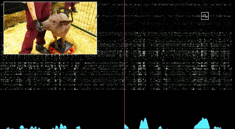
The horizontal lines of the graph represent the activity in each channel, white showing a group of neurons being active; the bottom is a summation of spikes across all channels at any given time.
More activity → Higher hill → Higher beeping pitch
Meanwhile, an average pig, a pig with removed Neuralink implant and pigs with multiple implants are also presented, demonstrating the link’s reversibility and safety.
Limb motion prediction in a strolling pig is showcased.
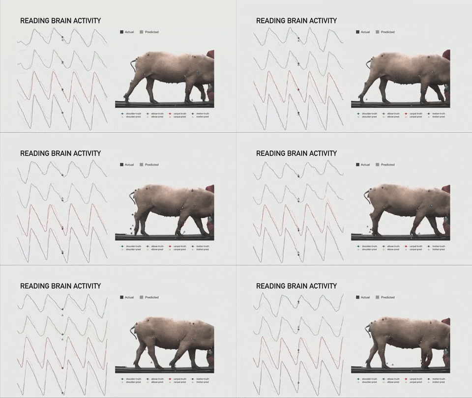
Some are skeptical towards the accuracy, which we’ll discuss in a bit.
However aside from that, not much can be extrapolated from this graph. The pig’s unique set of experiences relating to each straw can’t be decoded at the moment, as the storage site in the brain differs from pig-to-pig.
Monkey Mindpong
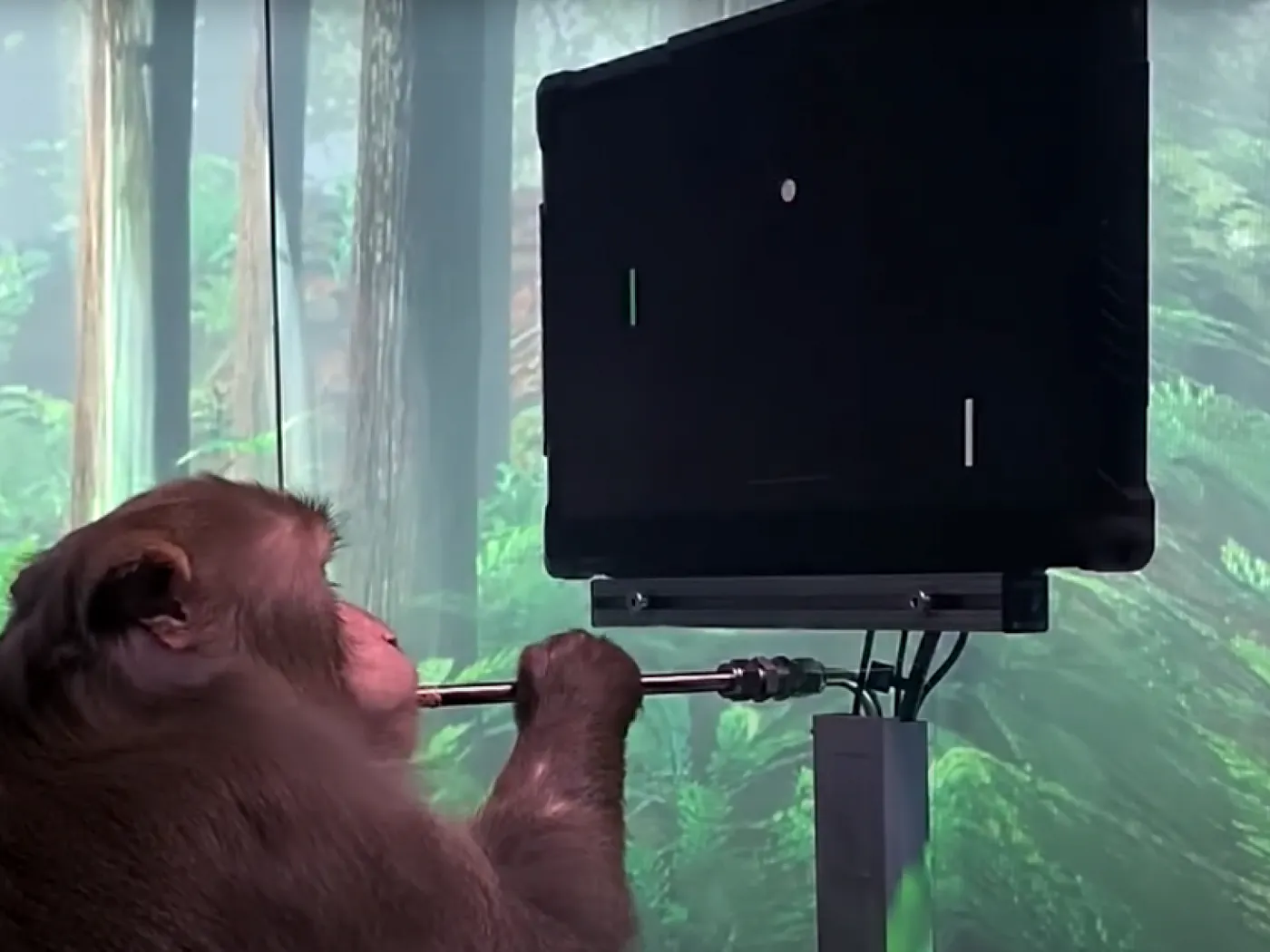
In April 2021, team Neuralink demonstrated a macaque monkey, Pager, playing pong directly from thought.
There are two N1 links placed across the left and the right motor cortex.
Again, calibration first. Pager used the joystick to guide a cursor to a targeted square while Link recorded neural activities. For example, activity in channel 8 might be correlated to intent for rightwards movement.

Pager calibrating the Neuralink implant
The number of spikes is sent to a computer with decoding software, which modelled the relationship between motor cortex activity to joystick movement.
Later, Pager can play pong relying on his brain activity and the decoder alone.
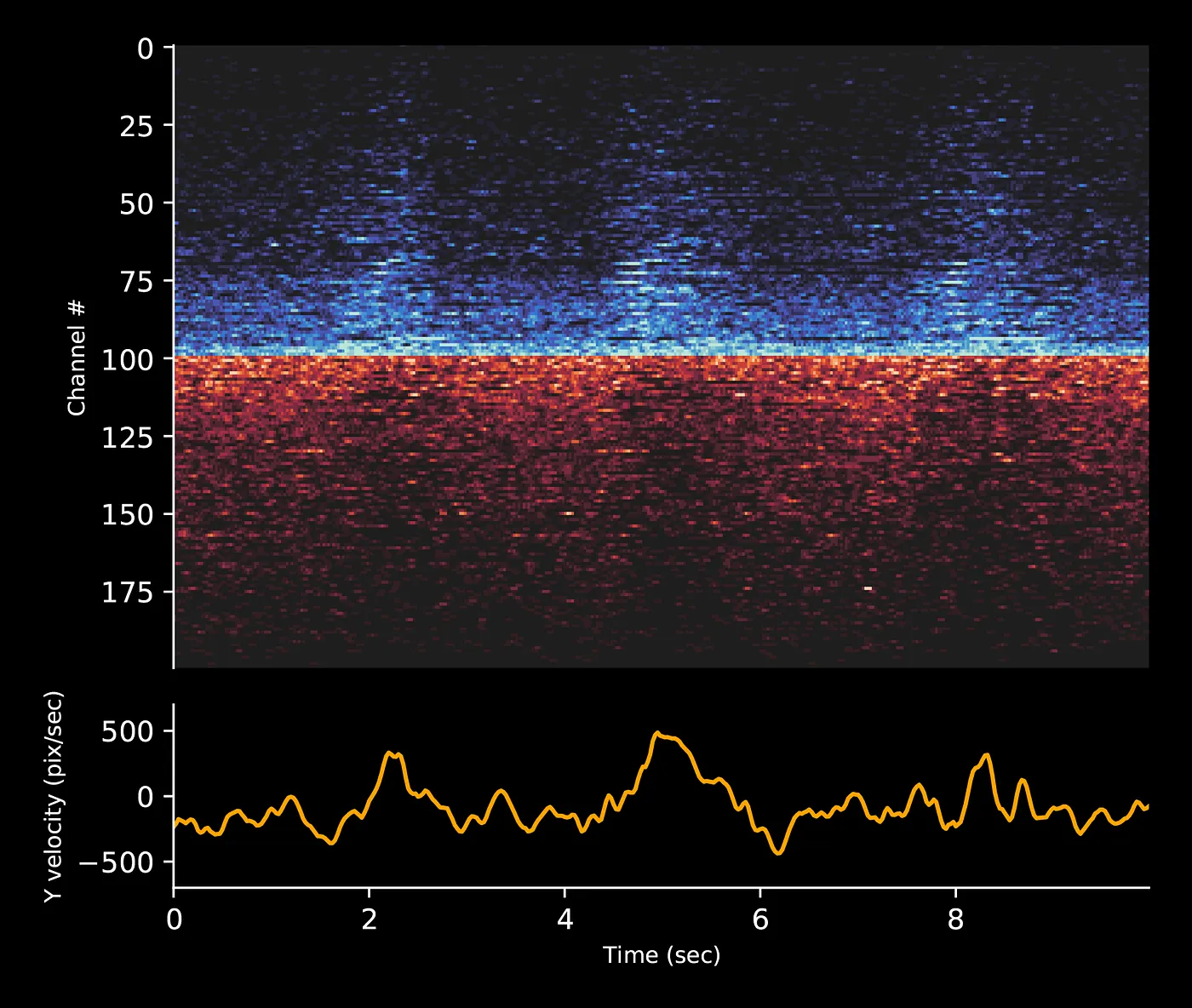
In the raster plot, the blue represents 100 channels with firing activity correlated to intended upwards movement. The red represents 100 channels with downwards movement. The firing intensity correlates to y velocity.
Stances on Neuralink
The majority of neuroscientists think that Neuralink is solid engineering but mediocre neuroscience.
Many lab BCIs have low bandwidth, implying that a very specific portion of the neurons needs to be trained to fire, largely unlike the fluency of everyday actions. Neuralink made lab products easier to use. Namely, installment ease, operating ease, bandwidth, latency, # of channels, easily generalizing the controls and the user’s physical comfort. As the chip is trying to save power, the algorithm’s accuracy is sacrificed a bit. Most agree that the robot is innovative. The bold vision and publicity can spark the next generation’s interest in BCIs, AI and neuroscience. Neuralink is based on existing work. For example, wireless implants in monkeys have been demonstrated in 2014. The limb prediction in the pig demonstration was similar to an algorithm in a semi-invasive BCI in 2013.
There are a few micro and macro challenges:
- As we move on to decoding higher-level thoughts, a greater number of areas become involved. How signals are relayed between brain areas is not well understood.
- There is no one-size-fits-all solution for brain or spine disorders. A blind person’s brain differs based on time elapsed. As time passes, the visual cortex rearranges into the role of responding to tactile and auditory tasks. The goal is to stimulate the right regions.
- On the other end, gaining control over small groups of neurons is difficult in stimulation.
For these three reasons, “better engineering”, referring to (a) increasing the number of electrodes, (b) deeper electrodes and (c) better robots might only serve so much. It is still uncertain how long the electrodes can last.
The Neuralink team can continue to explore the balance between battery and performance. A Ph.D. student commented that due to the small size of Neuralink, the motion prediction accuracy was worse than the Utah array, and it wouldn’t be useful for mind-controlled cursors. Similarly, a strolling pig’s motion is relatively easier to predict, compared to one that runs.
A few scientists are concerned about skipping peer review, while a Twitter user countered, if Tesla has been peer-reviewed, we will still be waiting to this day.
This raises the question, how effective is peer review? And other problems at the heart of the academic publishing scene. This will be covered later in the article.
Overall, Neuralink at the moment focuses on translation of existing academic results into industry.
7.5Applications of BCIs
7.5Applications of BCIs
Four main applications would be examined here.
Redesigning learning and notetaking
One word sums up our current education system: Approximations.

The education system is divided into years to approximate the student’s ability to learn. Then approximating streams are created — applied, academic, AP, enrichment, etc. Tests then again approximate knowledge gained.
BCIs, supplying much data, can shift us from approximation-based learning to massively individualized learning.
As of now, teachers can give BCI headsets to students. Upon authorization, teachers can gain focus level, memory and perception data; they can thus alter the lesson schedule, length and order.
Soon, AI algorithms would start to aid the teacher in measuring the length and structure of the lesson. Eventually, it would be fluent enough to design content on its own.
Student confusion can be measured in place of tests. Another function of tests is acting as certificates. A replacement for this could be publishing a hands-on project, an explainer video, mentoring a younger student, etc.
A personalized system like this would be extraordinarily enjoyable for students. This is also time and resource-efficient.
Learning involves taking notes, and BCIs again provide us with a shortcut.
A functional BCI notetaker is being able to read words from the brain at ~130 wpm, read commands to search for images and commands on how to connect the concepts together. This is uploaded onto a computer, can be queried and can be viewed by eye.
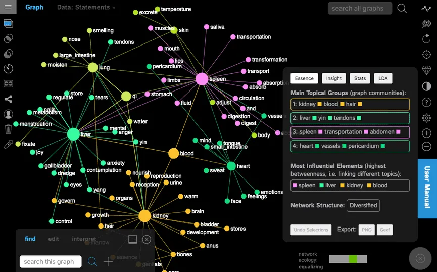
A genius BCI notetaker would involve reading words at a faster speed, autocompleting the mental scene, sketches and how the concepts are connected. A viewable version may not be necessary, as concepts could be directly beamed into the brain whenever the user wants. This is an example of Human-AI symbiosis.
Superior learning speed
If you learn a new language after 18, fluency would be troubling to maintain when immersion stops. This is thought to be related to declining neuroplasticity with age. Neuroplasticity refers to the brain reorganizing itself — the synapses being strengthened or weakened to fit new habits. A stronger synapse means more ions are allowed to enter the neuron’s membrane per time.
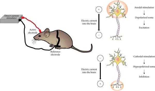
The two types of tDCS are Anodal and Cathodal, differing by the direction of charge flow to either excite or inhibit neural activity.
This shift can be sped up by using transcranial direct brain stimulation (tDCS), where a small current is applied externally to the scalp.
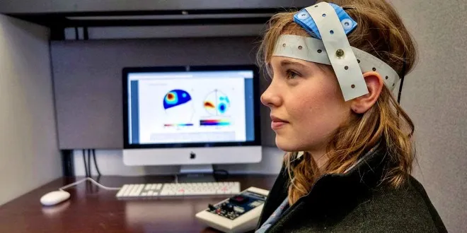
How tDCS could look like
Some study examples are accelerating the learning of social skills, math skills, motor skills and aiding a stronger memory.
However as this is still a nascent technology, there are risks of scalp burns. The changes are reversible, depending on how you think after the tDCS session. And tradeoffs exist, for example between skill acquisition and fluency of the skill.
** Smart workplaces**
This has been implemented by a Toronto startup, “Muse” as a corporate wellness program. Giving employees BCI headsets could monitor their attention levels, and thus adjust the workplace’s heating, humidity, CO2 and lighting. An employee’s current attention could be gauged and compared to the one needed for a meeting. Focus monitoring could help people decide when to take a break or to stab laziness in its face.
Everyone can be an artist
A person hears a tune in their head, but there is a barrier: insufficient music theory knowledge. This prevents them from recording the melody and composing.
YouTube lowered the entry barriers to content creation, Netflix for film watching, and Replit for programming. BCIs coupled with AI services could lower the entry barriers to almost all creative mediums.
A BCI can one day be used to capture a phrase of the mental song and inputted into AI music generators e.g. FlowMachines, IBM Watson beat, etc. to complete the tune. The user wouldn’t need to study music theory or composing software.
Similarly, in this video, a working webpage is created from a prompt made in English.
The MOMENT is a brain-controlled film made in 2018.

The watcher wears a NeuroSky MindWave headset that tracks attention levels. It is sent wirelessly to a computer to recombine the scenes as well as the background music. The film contains 17 scenes, the user being able to choose from 6 shots per time. Thus, you could watch 16,926,659,444,736 unique versions of it.
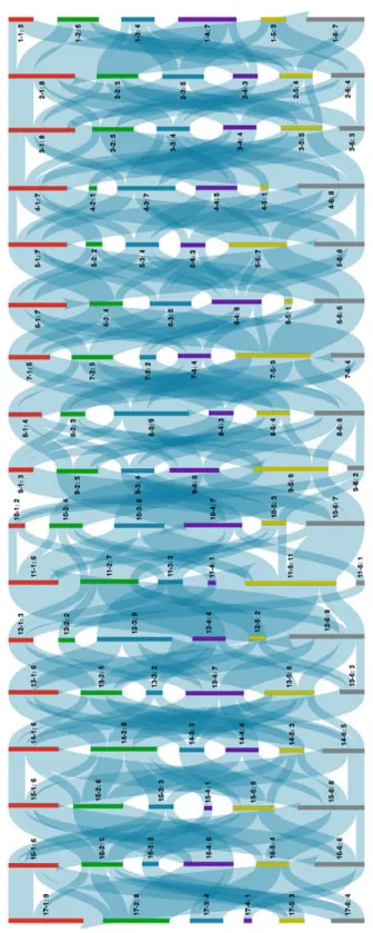
Unique journeys through 17 scenes of the film. Here’s another example in fashion.
Instead of picking clothing and shoes from a variety of approximated sizes, they can automatically fit you. BCI then comes into play by enabling personal aura projection. As you stroll down the street, your clothes change in colours.
This is the vision: We use BCIs to record neural activity, then integrate with AI to allow composing, writing, filmmaking, coding, drawing, fashion, metaverse homes, etc. The far future might even directly project emotions or senses to the audience in media.
As there are thousands of possibilities for BCI applications, an app store will almost certainly be built in the near future.
However, as there are few entry barriers and many producers, it becomes difficult to differentiate. Policies for allowed software should also be decided.
Everyone can become an artist, whether you are creating the rules, like the film director, or creating from the rules, like the audience.
Health Only 35% of adults in the US report sleeping on average more than 7 hours per night. This includes multiple wakes, poor quality and others. It is taxing on productivity and is correlated with obesity, type 2 diabetes, etc. Sleep is composed of four stages: stages 1–4, which are non-rapid eye movement (NREM) sleep as well as REM sleep. There is a distinct brainwave associated with each stage of sleep, as shown below.
A non-invasive headset with tDCS could be used to influence our brainwaves.
During NREM sleep, anodal stimulation is used to excite neuronal activity. In REM sleep, cathodal stimulation would be applied.
This is one of the aims of Neuralink. Sleeping efficiently could free up time in the coming decades. A 2016 study showed that sleep time could be reduced by 25 minutes.
Other popular use cases of BCIs involve patients controlling prosthetics and wheelchairs with their minds. This article won’t go into details as there are many writings on this.
Overall, BCIs shorten the bridge between ourselves and goals — learning, work, entertainment and health — allowing everyone to run across the bridge with higher efficiency.
Obviously, risks do exist, e.g.
- Is the decision made by the algorithm, or by the human?
- Who can access brain data?
People worry that BCIs make us less human. A similar question would be: Is the 10 or the 20 y.o. you more you?
Human values are constantly evolving. Imagine if we didn’t have computers, as some person argued that it makes us less human. As a result, Google, Youtube, Facetime may not have been developed to boost our work efficiency. There are tradeoffs and risks with every innovation, but the trend is that ideas breed more ideas to shadow misuses.
7.6How to accelerate BCI development
7.6How to accelerate BCI development
Advancing research in BCIs requires research in AI and neuroscience, as well as intersections with fields.
However, many researchers said the field looks more like:
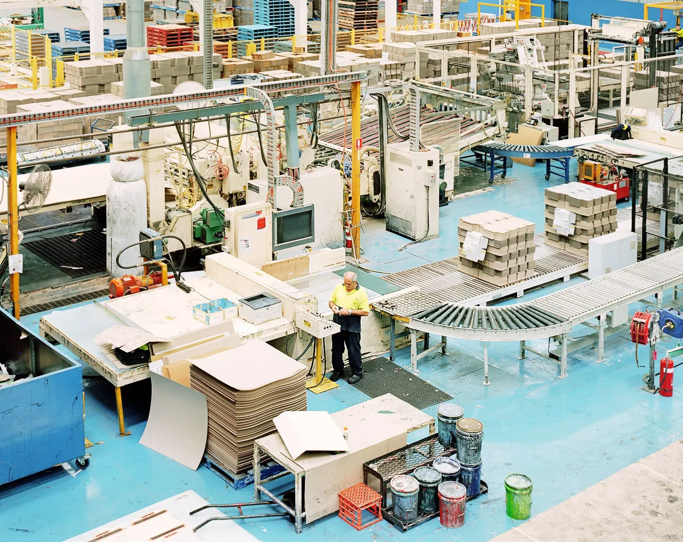
Paper factory at work!
To get funding, positions and fame, researchers are pressured to continuously publish papers, with the number of citations as an indicator of success.
This leads to exaggerating the paper’s importance, cramming in intellectual nonsense and sacrificing the overall quality.
A large volume of papers and no incentives cause peer reviewers to slack off — publishing papers that only align with contemporary views, allowing poor quality papers to appear, and occasionally harassing authors by telling them to make unnecessary edits.
Worse, journals and papers are ever-increasing in price. This limits the number of quality research in-game.
Here are a few remedies:
- Set up funds that require research done with the funding to have open access.
This is being implemented by the Bill & Melinda Gates Foundation. The model could also be used to set up BCI-specific funds, requiring software to be open source to spur collaboration. This accumulates free-to-read papers and code.
- Make research readable
a) Fermat’s library is a software that allows crowd annotation of papers. The founders also suggested publishing research in threads like on Twitter. b) Researchers could be given an exposition quota, where they must give a certain number of expository talks and nontechnical introductions to their research. Here’s an example of Tai-Danae Bradley’s Ph.D. thesis:
c) Expositions on existing research. A number of videos, games, blogs, etc. were created for the Summer of Math Exposition contest in 2021. At the present, there is a lack of tutorials in the field of BCIs. A “Summer of Neuro Exposition” could be similarly organized, as well as hackathons e.g. BR4IN.IO. That said, it is speculated that BCIs will grow spectacularly in 10 years.
In conclusion, Neuralink’s chip could read and write to the brain and aims to tackle disorders recently. It could be a key player in hyping up the BCI industry and accelerating the coming of sci-fi technology.
7.7Further reading
7.7Further reading
- Prediction of Three-Dimensional Arm Trajectories Based on ECoG Signals Recorded from Human Sensorimotor Cortex
- How Neuralink Analyzes Your Brain
- [Brain-Computer Interfaces for Artistic Expression])(https://link.springer.com/book/10.1007/978-3-030-14323-7)
Highlight 8Reviewing ultracold atoms and integrated photonics simulators! [note-0051]
- 09-01-2021
- Zheng Li, Chenxi Shi, noesis, Shuzhi Zhu
- #quantum-simulation
- #physics
Highlight 8Reviewing ultracold atoms and integrated photonics simulators! [note-0051]
- 09-01-2021
- Zheng Li, Chenxi Shi, noesis, Shuzhi Zhu
- #quantum-simulation
- #physics
8.1Abstract
8.1Abstract
With the development of quantum physics, quantum simulation technology has become more mature and has many applications in real life. This paper introduces two methods of quantum simulation: ultracold atom simulation and integrated photonic simulation. First, ultracold simulation is easy to observe and highly manageable, and its experimental results often agree with the theory. Besides these, it also has limitations. Thus, how to surpass the general theoretical simulation is essential in the future. Then for integrated quantum photonics, it is easy to manufacture, available at room temperature and allows long simulations with a high degree of experimental control. With a few components optimized, large-scale quantum photonic circuits with many photons can likely become a reality in the coming decade.
8.2Introduction
8.2Introduction
Since the early 20th century, quantum mechanics has become one of the most basic theories in the cognition of nature, a discipline to explore the physical laws of the micro world. The microscopic behavior of all physical systems or phenomena should meet the basic principles of quantum mechanics, so the simulation principle of any physical system should be based on quantum mechanics rather than classical physics. As the main content of quantum computing and quantum information science research, quantum simulation is to simulate and study the system that is unfamiliar or difficult to control by using a controllable quantum system.
Quantum simulation is a concept created by Feynman in 1982. To solve the problem that classic computers cannot simulate the quantum system accurately, Feynman suggested using a manageable quantum device to simulate the quantum behavior in other systems, which was the original motivation for the development of quantum computing, as quantum simulation has high requirements for computers with a large number of calculations [1]. For example, in quantum chemistry, classic computers cannot even simulate the behavior of molecules in median size. In condensed matter physics, quantum simulation is an ideal platform for research in a quantum phase transition and high-temperature superconductor (HTS) [2]. Methods for quantum simulation have sprung up in decades, and therefore a paper to summarize and compare the methods is necessary for the efficiency of future study. This paper summarizes two methods for quantum simulation, ultracold atom simulation and integrated photonic simulation. Firstly, for ultracold atom simulation, its reasons for being an ideal platform for quantum simulation, such as the considerable controllability of ultracold atoms, will be introduced, along with a discussion of the technical advantages of ultracold atom simulators challenging ideas. Then for integrated photonic simulation, it aims to combine photon sources, routing, optical processing and photon detectors on one chip for practicality, and its necessity in the quantum simulation will be demonstrated in this paper.
8.3Ultracold atom simulators
8.3Ultracold atom simulators
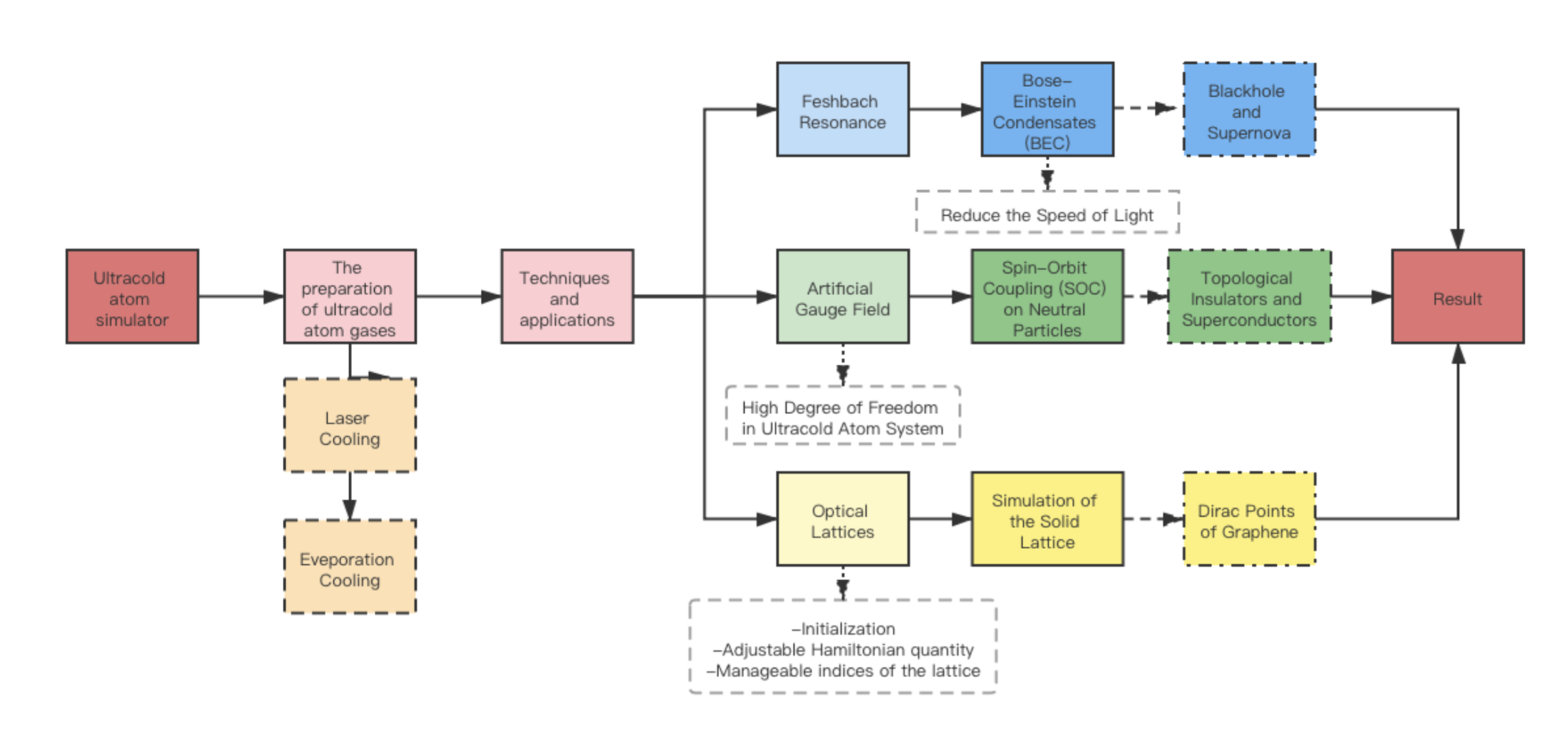 Figure 1. The mind map of this section.
The speed of atoms at room temperature is about 300 m/s [3]. However, there is a downward trend in the momentum of atoms with a decrease in temperature, and therefore an increase in de Broglie wavelengths of particles, according to the momentum equation and de Broglie relation in quantum physics $p=\frac{3}{2} kt$ and $λ=h/p$ when de Broglie wavelengths of atoms are the same as the distance between atoms, Bose-Einstein Condensates (BEC) forms, as shown in Figure 2 [4].
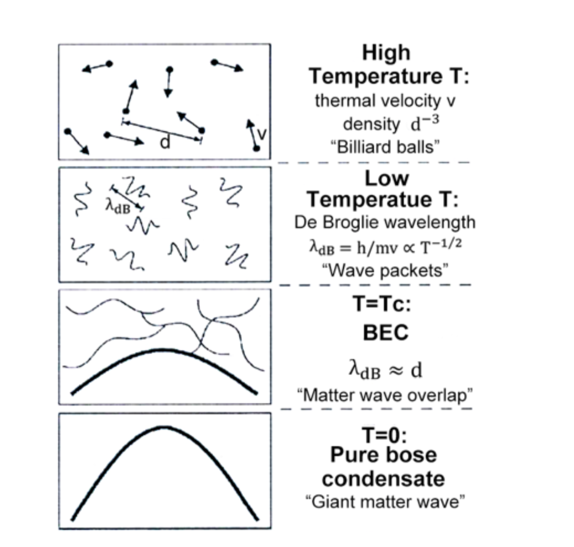 Figure 2. The formation mechanism of BEC [5]. Particles move like billiard balls at high temperatures. De Broglie wavelength and volatility of particles increase while temperature decreases, and therefore it moves like wave packets. At the critical temperature, or degeneracy temperature, de Broglie wavelength of atoms is the same as the distance between atoms, atoms interfere with each other, and BEC forms, with quantum effects like tunneling effects clearly shown in the behavior of atoms [6].
Ultracold atoms are defined as atoms at extremely low temperatures, usually in the magnitude of $10^{-3}$ - $10^{-9}K$. Ultracold atom gases are neutral and thin, whose density is usually in the magnitude of $10^{13}-10^{15}cm^{-3}$ [4]. At a low temperature, the elastic and inelastic scattering of particles is controlled by quantum mechanical effects such as resonances or tunneling through barriers since the de Broglie wavelength becomes comparable to the range of the interparticle interactions. Prominent quantum effects, combined with high purity and high handling of electromagnetic fields, make ultracold atoms an ideal platform for quantum simulation.
The ultracold atom system is highly manageable. In solid materials, the internal structure is fixed by the rigid structure of materials. In contrast, in ultracold atom experiments, factors like the dimensions of the potential well, indices of the light field, number of atom gases, temperature, and the strength of the magnetic field can all be regulated according to the requirements of the experiment [7]. This is how quantum simulation is done in subsections.
Preparation of ultracold atom gases.
Preparation of ultracold atom gases needs the combination of many sets of technology. In the procedure, atoms are made cooled and trapped by the laser and evaporation cooling technique and the magnetic trap. The key of the first step is the Doppler cooling and Zeeman effect. The Zeeman reducer coordinates with a magneto-optical trap in this step. As atoms gain and lose kinetic energy respectively when transmitting and absorbing photons, it receives recoil force from photons. According to the Doppler effect, the frequency of incident light sensed by atoms with different speeds is different, and therefore they receive force with different magnitudes. Thus, regulating the incident frequency in different directions and altering atoms' resonant frequency according to the Zeeman effect, a force opposite to the direction of atomic motion exerts on atoms to decrease the speed of atoms.
Consequently, atoms can be trapped by the magneto-optical trap, and a further step of Doppler cooling makes the temperature of atoms down to approximately 100 μK. However, there is a lower temperature limit for the laser cooling technique, as the spontaneous radiation can warm up the atoms. In the second step, the evaporation cooling technique enables the atoms with relatively high energy to escape the system, lower the average energy level of atoms left, and therefore degeneracy temperature is reached, and BEC forms [8].
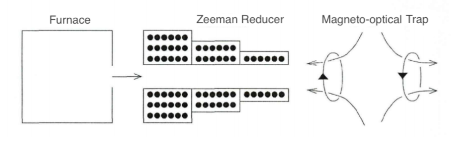 Figure 3. A typical experiment to cool and trap atoms.
The timeline in figure 4 shows the time point when some important ultracold quantum degenerate gases are realized, meaning that after decades of development, the technique to prepare ultracold atom gases is quite mature.
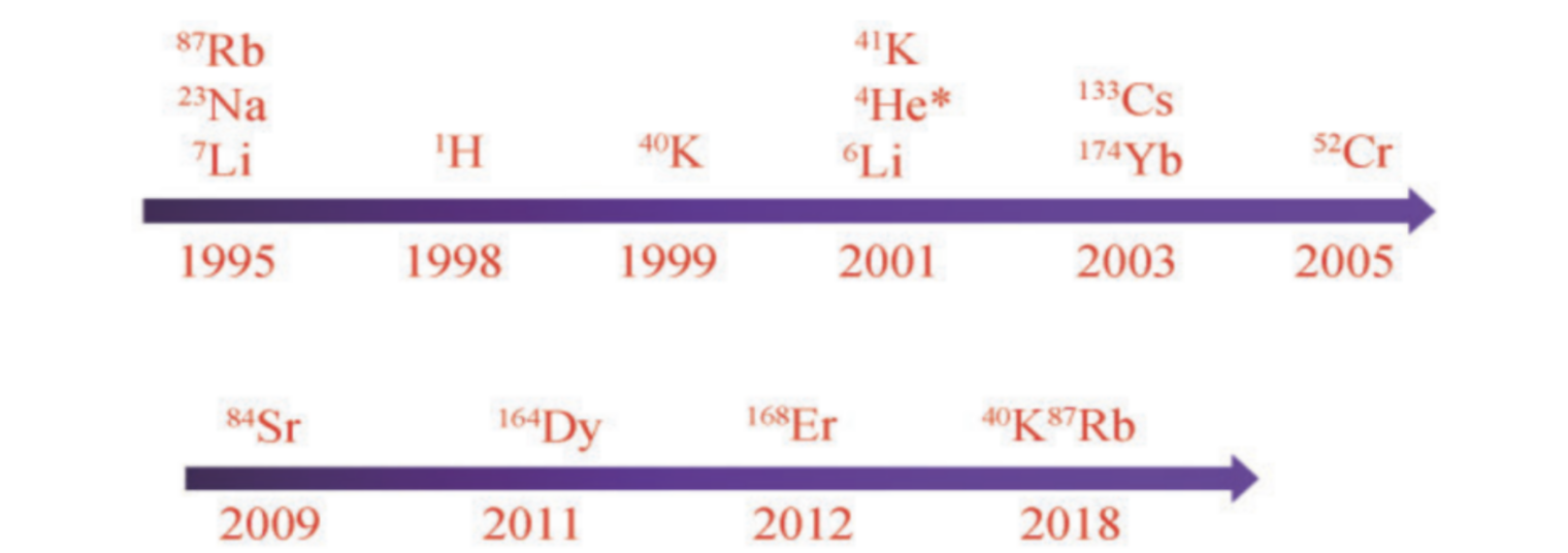 Figure 4. The timeline of the realization of important ultracold atom degenerate gases [9].
2.2 Bose-Einstein condensates and Feshbach resonance
The BEC is a gaseous, superfluid matter of a boson atom whose temperature is close to absolute zero. Almost all atoms are concentrated in the quantum state with the lowest energy, forming a macroscopic quantum state [10]. BEC has volatility and coherence like lasers, so interference between two laser beams can also occur between two condensates, observed by W. Ketterle [11]. Figure 5 shows the interference between two condensates, with a slit clearly shown. The properties of the wave and the unique state of matter explain why BEC is a good media for quantum simulation [5].
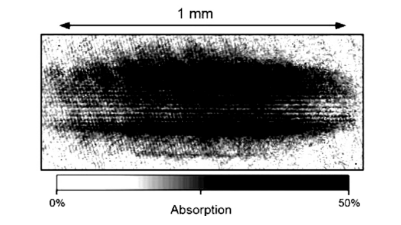 Figure 5. The interference observed by Professor Kettlerle between to BECs.
BEC has a high optical density difference. Lasers can change the state of atoms in the condensates so that there is a sudden increase in the refractive index of condensates, and the speed of light drops immediately, even to several meters per second. That is why BEC can be made a model for a black hole, as light is "frozen" in the condensate [12].
Thus, the unique properties of BEC make it ideal for lots of research in quantum physics and applications. In a closed channel, the atomic motion is constrained, and the channel wave function gradually disappears at infinity, while in an open channel, the atomic motion is not constrained, and the channel wave function oscillates at infinity asymptotically. The typical s-wave scattering length of alkali metal atoms is between 50 and 100 Bohr radii, and the distance between atoms is about 1.4 Bohr radii. In comparison, the interaction between atoms is very weak. Through Feshbach resonance, people can use the magnetic field to adjust the scattering length of the ultra-cold atoms in the open channel, and therefore adjust the strength of the interaction between the atoms. Feshbach resonance is an important technique for the simulation [7].
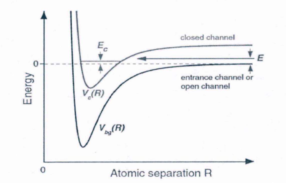 Figure 6. The diagram of the Feshbach resonance. By adjusting the energy difference between the open channel and the closed channel, the atoms in the open channel can undergo a resonance process with a divergent scattering length [4].
The application of Feshbach resonance benefits from the advent and development of the optical trap. Ultracold atoms are trapped in the optical trap, and therefore they escape from the attraction of the magnetic field. Feshbach resonance provides a method to adjust the external magnetic field so that the strength of particle interaction can be regulated artificially [13]. The transformation from BEC to Bardeen-Cooper-Schrieffer (BCS) superfluid is realized by regulating the interaction intensity between fermions. This technique can simulate the outburst of the supernova and black hole in BEC, control the generation of solitons, etc.
2.3 Spin-orbit coupling and artificial gauge field
In condensed matter physics, spin-orbit coupling comes from the movement of electrons in the inherent electric field of the atom itself, which is the core content of the Spin Hall effect, topological insulation, topological superconductors, Majorana fermions, spintronics, etc. Besides, it can also be extended to quantum computing [3].
It is mentioned above that ultracold atoms are electrically neutral. However, SOC merely exists on charged particles in the natural world. That is why the research of SOC only applied to the fermion system in the past, while the research on the boson system, which is the majority in the real world, was nearly empty. However, this limitation is removed in the artificial gauge field, with the interactions between atoms and light being regulated. In other words, spin-orbit coupling (SOC) on neutral particles is realized. It was first realized in 2009 by Spielman [14].
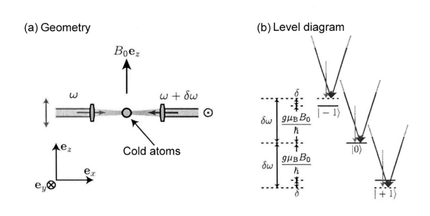 Figure 7. (a) General experiments with two light beams, (b) The energy level structure of three-energy-level atoms in the experiments.
Figure 7 shows the basic idea of Spielman's method. The particles considered in the methods are alkali metals Rb-87 and K-40, whose electron structure in the ground state is $2S_{1/2}$. Two back-propagation Raman laser beams trigger this kind of SOC along the x-axis, combined with a magnetic field on the z-axis. For one of the two laser beams, $\pi$, its polarization direction is along the z-axis, while for the other one, $\sigma$, it is along the y-axis. With the two laser beams, a biphotonic process is experienced by atoms. First, the photons are absorbed, and the particles are excited to the intermediate state $2P_{1/2}$ and $2P_{3/2}$. Then a photon in another type is transmitted so that atoms return to the ground state [15]. With indices flexibly changed in the ultracold atom system, the condition hard to reach in the real solid materials can be simulated, and new phenomena can be discovered. A typical example of this is topological insulators and topological superconductors.
2.4 Optical lattices
In the solid lattice, the distance between atoms is small, and therefore the interactions between atoms are great. On the contrary, the distances between lattice points and atoms are large in the optical lattice, so the interactions are small. As a result, particles' dynamical property and time evolution in the optical lattice are very slow compared to the solid lattice. However, the mode of motion and equations of motion of atoms in the optical lattice are similar to that of electrons in the solid lattice. Thus, using BEC in the optical lattice to simulate the solid lattice system is feasible. Phenomena that are hard to be observed in the solid, such as the Bloch oscillation, nonlinear Landau-Zener tunneling, etc., can be observed in the optical lattice. In addition, simulation of the complicated model in the condensed matter and the optical system can be realized as the optical lattice technique. The detailed calculations can be found in the review.
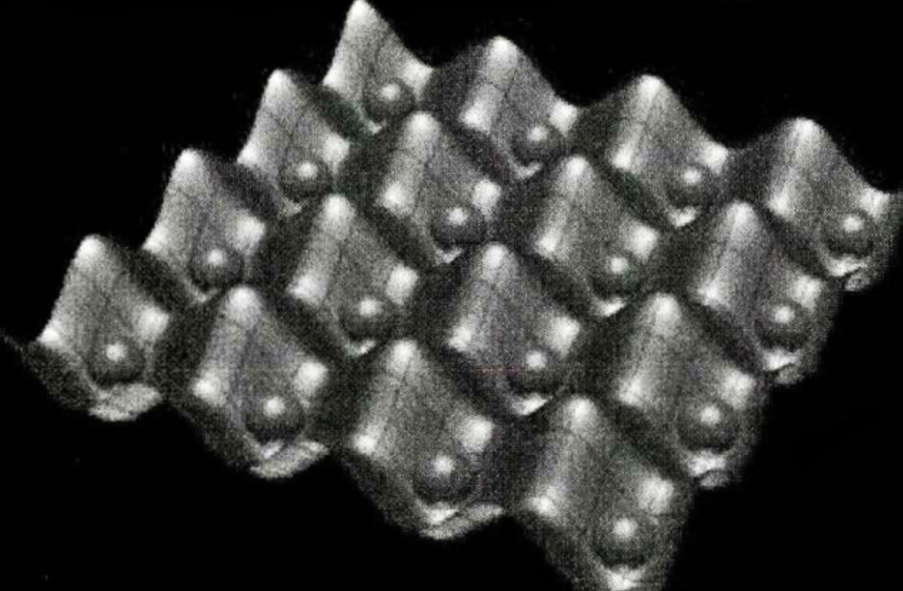 Figure 8. The general model of optical lattices [14].
The optical lattice is mainly realized by the AC stark effect between light and atoms. A periodic potential well is obtained using overlapping laser interferences in the optical lattice. The system can realize the initialization of many particles by using the existing experimental technology; the Hamiltonian quantity is also easy to adjust; by regulating the potential field of the optical lattice, the lattice structure and dimensions can also be changed. By adjusting the direction, quantity, angle, polarization, and frequency difference of the incident laser beams, a variety of 1-dimensional, 2-dimensional, and 3-dimensional optical lattices can be realized, and different potential fields can be added to the original optical lattice, thereby realize the quantum simulation of various Hamiltonian [16].
In a typical condensed matter system, electron motion can be seen as the lattice produced by the nucleus, which can be simulated by the optical lattice technique in an ultracold atom system. Take graphene as an example, one of the most promising materials in many fields, with electrical conductivity and strength. With the help of the optical lattice technique, Dirac points, the important structure in the graphene, can be simulated in the ultracold atom gas. Dirac points are the core of numerous new physics phenomena like the massless electrons in the graphene and the conductive boundary state of the topological insulation.
2.5 Results
The great achievements of the quantum simulation obtained in the decade have benefited from the favorable quantum nature of the ultracold atoms. Additionally, the optical lattice technique is also a key factor. The Feshbach resonance made the research on the intersection of BEC and BCS possible, and therefore the simulation of the complicated physical system like black holes, boosting the astronomy research. The artificial gauge field broke the limit that the ultracold atoms are neutral and realized the SOC on the boson system, filling the gap in this field. The research of aggregating dimensions can be seen as an expansion of the optical lattice, bringing new ideas for future research in quantum simulation.
Due to the purity of ultracold atoms, experimental results often agree well with the theory. Therefore, quantum simulations of ultra-cold atoms are often criticized as repeated verifications of theories. Nonetheless, while achieving great results in ultracold atom quantum simulation, we also see its limitations and bottlenecks. Thus, how to surpass the general theoretical simulation is a key point in the study of ultra-cold atom quantum simulation. The interaction between atoms makes our research work beyond the general single-particle image and enter the field of multi-body physics. This is a feature and advantage of ultra-cold atom quantum simulation and an important aspect of its scientific significance. Finding a new foothold is the key to development. In recent years, topological quantum simulation research has developed rapidly in ultracold atomic systems, which is an important direction. But at the same time, we must also see that topological quantum simulation is also developing rapidly in systems such as phonons and photons. In addition, in recent years, the direction of quantum computing has been greatly developed, especially the superconducting qubit system, which has greatly improved its quantum simulation capabilities. In addition, in recent years, the direction of quantum computing has been greatly developed, especially the superconducting qubit system, which has greatly improved its quantum simulation capabilities [9].
8.4Integrated Quantum Photonics
8.4Integrated Quantum Photonics
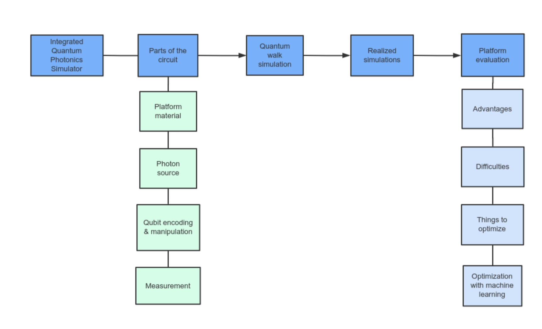 Figure 9. The flowchart of this section
Integrated quantum photonics aims to combine photon sources, routing, optical processing and photon detectors on one chip for practicality.
3.1 Parts of the circuit
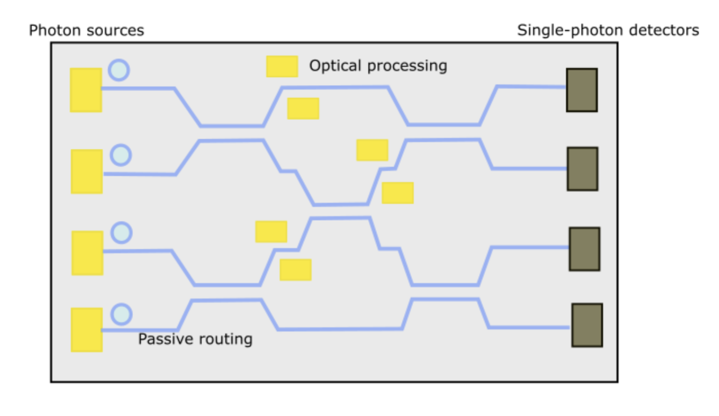 Figure 10. The scheme of an integrated quantum photonic circuit.
3.1.1 Platform material.
Due to the variety of optical components involved, various materials can be used as the substrate. For example, LN, GaAs, and InP are materials whose electro-optical effects allow fast manipulation of single-photon states. At the same time, silicon waveguides(the photonic equivalent of a wire) can keep light well confined with silicon's high refractive index, layered on silica [17, 23]. A higher index contrast allows smaller optical components.
3.1.2 Photon source.
Integrated quantum photonics relies on single-photon sources on the circuit. A single photon can be generated when a laser pulse strikes a particular type of semiconductor aka a quantum dot. Presently, the best performance is achieved by self-assembled InGaAs/GaAs materials [17]. Likewise, a pair of entangled photons can be generated via a crystal, such that depending on the input photon's polarization, two output photons will either share identical or orthogonal polarizations [18]. (see figure 2) Many other processes including the spontaneous four-wave mixing process can be used to polarize photons, with two photons being inputted.
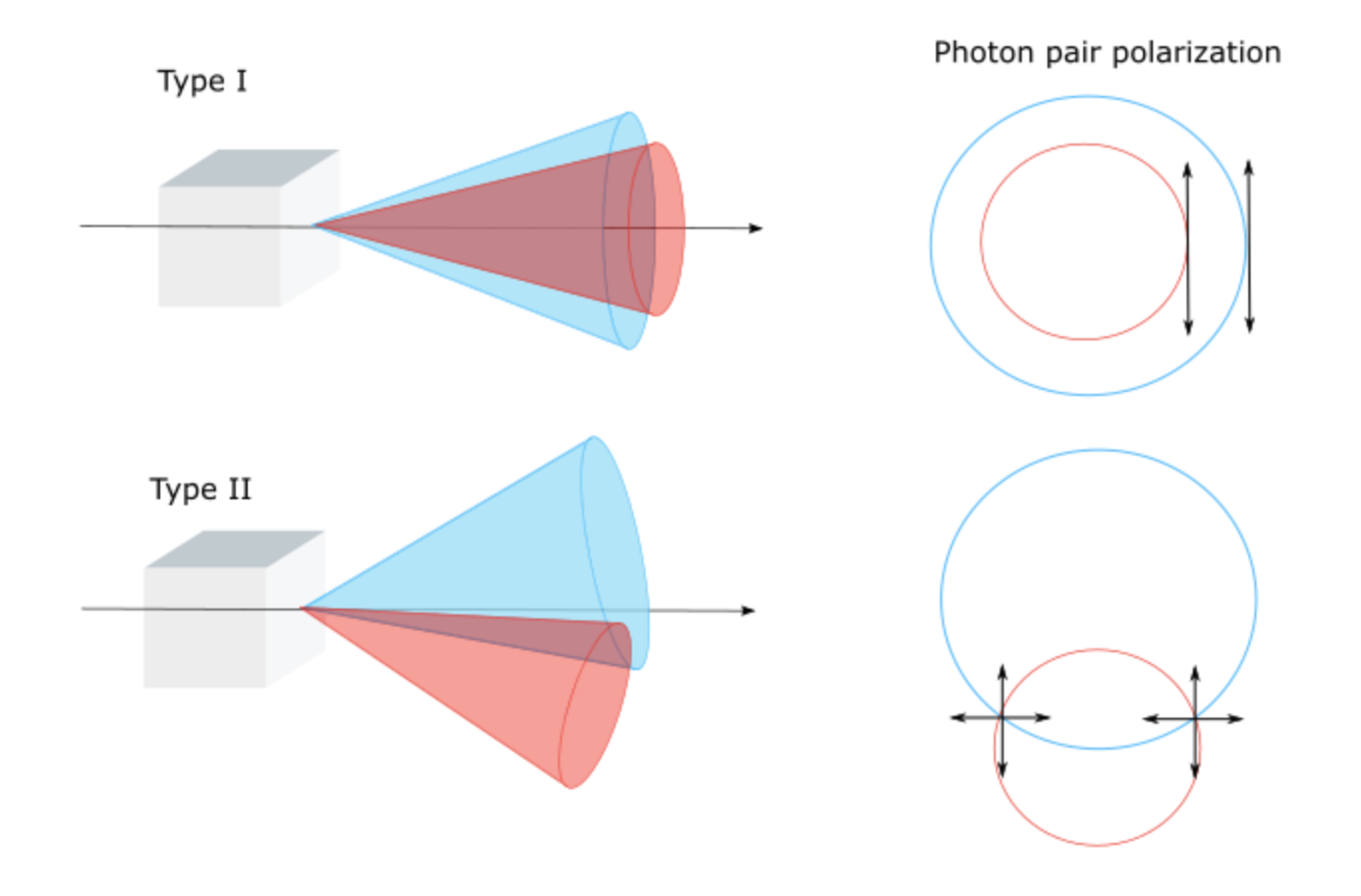 Figure 11. Parallel(Type 1) and orthogonal(Type 2) polarizations of entangled photons generated in the process of Spontaneous Parametric Down Conversion.
3.1.3 Qubit encoding and manipulation
Input variables in an algorithm are often encoded in the path, polarization, time of the single-photon, though many other methods exist [19].
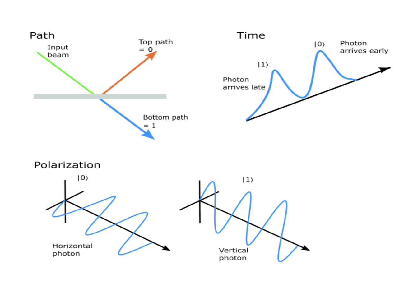 Figure 12. The three main types of photons encoding.
Photons are routed through the circuit by silicon waveguides, and when two waveguides come close together, they can form directional couplers that effectively divide light. Some examples of directional couplers are power splitters, polarization splitters and wavelength (de)multiplexers. Aside from the above passive elements, there are active elements that reconfigure the circuit. For example, phase shifters controlling phases of interferometers; polarization transformers and space switches acting as tunable beam-splitters. These active elements cannot be expected to operate identically in each use. Thus, they are a source of stochastic noise [20]. If multiple substrates are used, it is necessary to have interfacing components such as fiber waveguide coupling and dielectric mirrors.
3.1.4 Measurement
Quantum information is eventually read out by on-chip single-photon detectors (SPDs). One such technology uses a superconducting nanowire for detection. A superconductor carries electricity without friction, yet there is still a limit on the current passing at once. In SNSPD, a segment of the wire is charged with maximum current, such that when a photon passes by, it causes a decrease in the current limit, leading to a short loss of superconductivity. This change creates an electrical signal to record the passing photon [21].
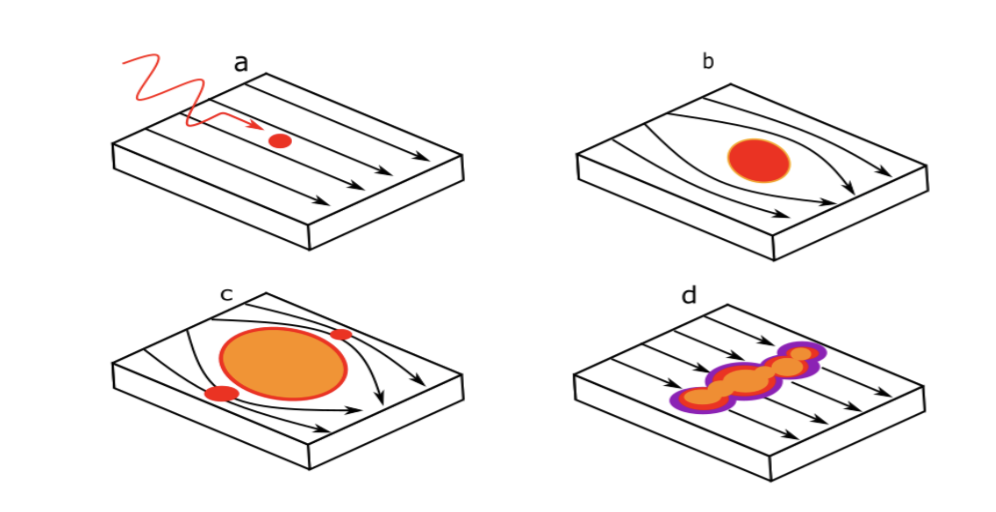 Figure 13. a. A photon enters the nanowire, creating a hot spot
b. Superconductivity is disrupted
c. A resistive region starts to span the entire region of the nanowire
d. A measurable voltage is induced across the device
Figure 13. a. A photon enters the nanowire, creating a hot spot
b. Superconductivity is disrupted
c. A resistive region starts to span the entire region of the nanowire
d. A measurable voltage is induced across the device
SNSPDs can achieve high detection efficiency. However, the chip needs to be placed in a cryostat containing, e.g., liquid helium [22].
Another detector, transition-edge sensors, has higher efficiencies, limited speeds and must be cooled to millikelvin temperatures for operation. Similarly, silicon avalanche photodetectors have a moderate efficiency but are significantly low speed [23]. Still, many quanta photonic functions are integrated with electronics to provide DC power, control and I/O with the classical world [2].
3.2 Quantum Walk Simulation
Photonics is an exceptional platform for performing large-scale quantum walks. A walk is a distribution occurring over a given graph following a defined equation of motion [24]. A quantum walk model describes the coherent propagation of quantum particles in networks [25]. (see figure 14.)
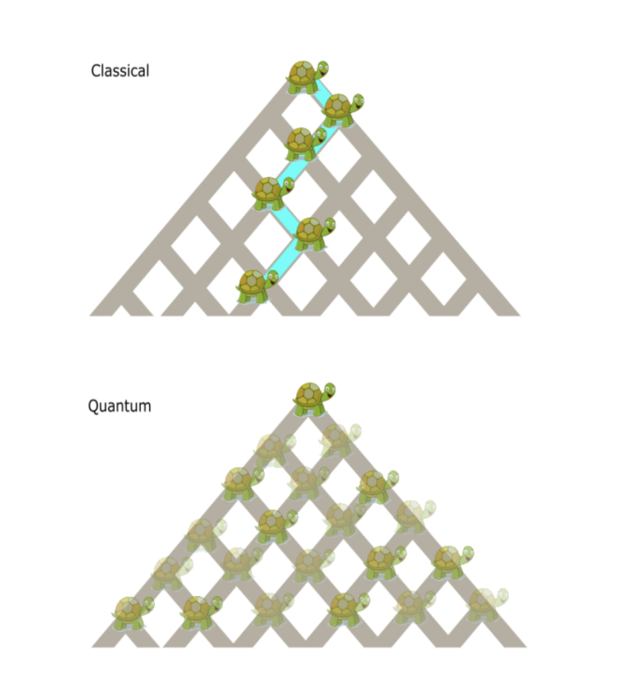 Figure 14. Comparing classical walks with quantum walks
The quantum walk is a powerful tool: It could explain energy transport in photosynthesis; emulate Darwinian evolution, quantum biophysics, systems with properties beyond standard models; solve isomorphism problems, realize universal quantum computation and build quantum algorithms [26, 28]. The well-known Grover's search algorithm can be viewed as a quantum walk algorithm [27]. Similarly, the computation for the boson sampling problem, which is essentially asking, "What is the distribution of photons?" can be massively simplified by running on a quantum photonic device and is key in demonstrating quantum advantage with current technology [29].
Due to the long coherence times of photons, long evolutions of quantum walks can be simulated while giving a high degree of experimental control. One technique using femtosecond lasers can draw precise three-dimensional waveguide networks within the glass. As the third dimension is used to propagate the wave, this allows the simulation of two-dimensional quantum walks [28].
In the past decade, demonstrations ranged from single particles walking on two-dimensional lattices to multiple particles interfering on one-dimensional structures to multiple photons evolving on a two-dimensional platform [26]. They have been simulated using bulk optics and waveguides.
3.3 Realized simulations examples
Molecules can be simulated using near-term devices. In 2018, the eigenvalues of the ground and excited states of molecules, e.g., hydrogen was approximated on a programmable silicon photonic chip, using a combination of quantum phase estimation and variational eigensolver [22]. The results were estimated with 32 bits of precision with fidelities > 99%. The vibrational dynamics of four-atom molecules, e.g., ammonia, sulfur trioxide, energy transport in a protein fragment and a water molecule reaching thermal equilibrium were simulated [37]. Simulations can be evaluated using Hamiltonian learning, where a small, trusted quantum simulator verifies a large untrusted one [31]. In 2020, a quantum advantage was demonstrated on the bulk photonics quantum computer Jiuzhang by implementing a type of Boson sampling with 76 photons [29].
3.4 Platform evaluation.
Integrated quantum photonics is a promising candidate in simulating complex systems. The speed of photons allows interaction between a large number of components that are already supported by the mature CMOS fabrication process, providing the basis for scaling up [20]. The current classical PICs contain thousands of components in a few microns, but millions of components may be contained in the future [20]. The platform can run at room temperature and does not need to be isolated, reducing costs. Since photons do not interact with the environment easily, they have close to maximum-possible coherence time meaning many operations can be performed [20].
However, this non-interactive property also implies difficulty in making two-qubit gates, which are key in realizing universal quantum computing in the gate-based approach. Extreme devices such as the ultra-high-Q resonators are used, generating massive overhead, and the gate-based approach is considered impractical for scaling up [32].
In the one-way quantum computing approach, the difficulty presents in generating multiphoton entangled states in a relatively easy-to-implement circuit [30]. This approach is widely considered more realistic.
Currently, eight photons can be generated and processed in the same silicon chip [33]. Constructing devices with many qubits requires efficient single-photon sources, generating multiphoton entangled states that travel in a network of low-loss optical switches or waveguides. These are foundational to a fault-tolerant quantum computer. Once a sufficient number of photons are available, slight qubit loss will be sufferable, as the information can be recovered by applying Topological Error Correction [30]. Presently, photon counters are the only components that operate at cryogenic temperatures. By developing room-temperature photon counters, completely integrated photonic chips are possible. The room-temperature advantage can then be fully exploited.
In the near term, machine learning could speed up the design and experimental process.
For instance, a model was recently shown to recognize and select pure photon emitters with 95% accuracy and is 100 times faster than the conventional method [34]. Similarly, learning models are shown to have designed experiments more efficiently than the best previous approaches while rediscovering experimental techniques that are only recently becoming standard in quantum optical experiments [35]. Chip imperfections arising from manufacturing could be mediated with a combination of machine learning and on-demand programming of the chip [17]. Finally, machine learning could be used for validating quantum simulation data [36].
With these challenges solved, large-scale quantum photonic circuits with many photons can probably be used for simulation in the next decade.
8.5Conclusions
8.5Conclusions
Quantum computing and quantum simulation develop very fast; numerous achievements and new applications have spawned. This paper makes an overview of the past achievements of quantum simulation.
The advantage of ultracold atom simulators is the flexibility and purity, simulating the especially complicated physical cases and producing results with a high theoretical agreement. However, the future challenge in this field is to improve the uniqueness of the simulator since other techniques in quantum computing and simulation like superconducting quantum computers with high qubit numbers. This paper suggests that the key points of this are to lower the cost of material preparation and simulation and enlarge the range of cases and models it can simulate.
Likewise, the features of integrated quantum photonic simulators are the feasibility of manufacturing, the speed and the long coherence times of the qubit. The device can operate at room temperature except for one component. Much effort is needed to integrate this component onto a room-temperature chip and optimize several other processes, which can be aided by machine learning.
Those technologies may be used in many aspects in the future, and there are still some obstacles that need to be overcome. Through this, we hope more people can understand and interest in quantum simulation, and there will be more remarkable advances and amazing applications in the future.
References
[1] Feynman R P. Simulating physics with computers. International Journal of Theoretical Physics, 1982, 21(6): 467-488.
[2] Georgescu I M, Ashhab S, Nori F. Quantum simulation. Review Modern Physics, 2014, 86(1): 153-185.
[3] Shen X 2018 Quantum Simulation and Detection of Topological Invariant in Ultracold Atom System D. University of Nanjing
[4] Pan J 2017 Quantum Simulation with Ultracold Atoms D. University of Science and Technology of China
[5] Ketterle W. Nobel lecture: When atoms behave as waves: Bose-Einstein Condensation and the atom laser. Review Modern Physics, 2002, 74(4): 1131-1151
[6] Staanum P, Kraft S D, Lange J, Wester R and Weidemüller M 2006 Experimental Investigation of Ultracold Atom-Molecule Collisions J. Physical Review Letters 96(2). doi:10.1103/physrevlett.96.023
[7] Peng P and Gao C 2020 The history of ultracold atoms J. Science. 72(01): 41-46+4
[8] Deng T 2019 Quantum Control in Ultracold Atomic Gases D. University of Science and Technology of China
[9] Yan B 2021 Quantum simulation based on ultracold atoms in a lattice J. Physics 50(01):31-36
[10] Han Z 2019 The Study of Numerical Method Based on Bose-Einstein Condensate D. Shenyang Normal University
[11] Xu Z, Li Y, Zhang X and Wu Z 2017 The physical exploration of Bose-Einstein Condensate J. Physical Experiment of College 30(03): 63-68.
[12] Zhou Z 2019 Coherent Control of Ultracold Atomic Regular and Chaotic Transport D. Hunan Normal University
[13] Feshbach H 1958 Unified theory of nuclear reactions J. Annals of Physics 5(4): 357-390
[14] Dong D 2015 Schemes in Cold Atoms about Quantum Simulation and Quantum Computation D. University of Science and Technology of China
[15] Goldman N, Juzeliunas G, Ohberg P and Spielman I B 2014 J. Rep. Org. Phys. 77126401
[16] Liu W, Zhou X, Jiang K, Liu L, Xia L, Li X 2019 Ultracold atom simulators based on artificial gauge field and the optical lattice J. China Basic Science 21(05):41-57.
[17] Spontaneous parametric down-conversion. (2021, March 16). Retrieved from https://en.wikipedia.org/wiki/Spontaneous_parametric_down-conversion
[18] What is a qubit? (2021, April 20). Retrieved from https://uwaterloo.ca/institute-for-quantum-computing/quantum-101/quantum-information-science-and-technology/what-qubit
[19] Rudolph, T. (2017). Why I am optimistic about the silicon-photonic route to quantum computing. APL Photonics, 2(3), 030901. doi:10.1063/1.4976737
[20] Kingery, K. (2017, December 15). Single-photon detector can count to four. Retrieved from https://phys.org/news/2017-12-single-photon-detector.html
[21] Pernice, W., Schuck, C., Minaeva, O. et al. High-speed and high-efficiency travelling wave single-photon detectors embedded in nanophotonic circuits. Nat Commun 3, 1325 (2012). https://doi.org/10.1038/ncomms2307
[22] Santagati, R., Wang, J., Gentile, A. A., Paesani, S., Wiebe, N., Mcclean, J. R., . . . Thompson, M. G. (2018). Witnessing eigenstates for quantum simulation of Hamiltonian spectra. Science Advances, 4(1). doi:10.1126/sciadv.aap9646
[23] Moody, G., Sorger, V., Juodawlkis, P., Loh, W., Sorace-Agaskar, C., Jones, A. E., . . . Vidarte, L. T. (2021). Roadmap on integrated quantum photonics. Journal of Physics: Photonics. doi:10.1088/2515-7647/ac1ef4
[24] Aspuru-Guzik, A., Walther, P. Photonic quantum simulators. Nature Phys 8, 285–291 (2012). https://doi.org/10.1038/nphys2253
[25] Department Physik - Quantum Walks (Universität Paderborn). (n.d.). Retrieved from https://physik.uni-paderborn.de/silberhorn/forschung/quantum-networking/quantum-walks
[26] Jiao, Z., Gao, J., Zhou, W., Wang, X., Ren, R., Xu, X., . . . Jin, X. (2021). Two-dimensional quantum walks of correlated photons. Optica, 8(9), 1129. doi:10.1364/optica.425879 [27] Quantum walk. (2021, June 10). Retrieved from https://en.wikipedia.org/wiki/Quantum_walk
[28] Gräfe, M., Heilmann, R., Lebugle, M., Guzman-Silva, D., Perez-Leija, A., & Szameit, A. (2016). Integrated photonic quantum walks. Journal of Optics, 18(10), 103002. doi:10.1088/2040-8978/18/10/103002
[29] Garisto, D. (2020, December 03). Light-Based Quantum Computer Exceeds Fastest Classical Supercomputers. Retrieved from https://www.scientificamerican.com/article/light-based-quantum-computer-exceeds-fastest-classical-supercomputers/
[30] Slussarenko, S., & Pryde, G. J. (2019). Photonic quantum information processing: A concise review. Applied Physics Reviews, 6(4), 041303. doi:10.1063/1.5115814
[31]Wiebe, N., Granade, C., Ferrie, C. & Cory, D. G. Hamiltonian learning and certification using quantum resources. Phys. Rev. Lett. 112, 190501 (2014).
[32] Chen, Z., & Segev, M. (2021). Highlighting photonics: Looking into the next decade. ELight, 1(1). doi:10.1186/s43593-021-00002-y
[33] Wang, J., Sciarrino, F., Laing, A. et al. Integrated photonic quantum technologies. Nat. Photonics 14, 273–284 (2020). https://doi.org/10.1038/s41566-019-0532-1
[34] Kudyshev, Z. A., Shalaev, V. M., & Boltasseva, A. (2020). Machine Learning for Integrated Quantum Photonics. ACS Photonics, 8(1), 34-46. doi:10.1021/acsphotonics.0c00960
[35] Melnikov, A. A., Nautrup, H. P., Krenn, M., Dunjko, V., Tiersch, M., Zeilinger, A., & Briegel, H. J. (2018). Active learning machine learns to create new quantum experiments. Proceedings of the National Academy of Sciences, 115(6), 1221-1226. doi:10.1073/pnas.1714936115
[36] Biamonte, J., Wittek, P., Pancotti, N., Rebentrost, P., Wiebe, N., & Lloyd, S. (2017). Quantum machine learning. Nature, 549(7671), 195-202. doi:10.1038/nature23474 [37] Sparrow, C., Martín-López, E., Maraviglia, N. et al. Simulating the vibrational quantum dynamics of molecules using photonics. Nature 557, 660–667 (2018). https://doi.org/10.1038/s41586-018-0152-9